
Sapphire substrates provide excellent hardness, thermal stability, electrical insulation and chemical resistance. These properties make sapphire an important substrate for GaN epitaxy, LEDs, optical devices, sensors and other semiconductor applications.
However, sapphire is also a hard and brittle single-crystal material. Small chips, cracks or grinding damage near the wafer edge can expand during handling, high-temperature epitaxy, coating, thinning or dicing.
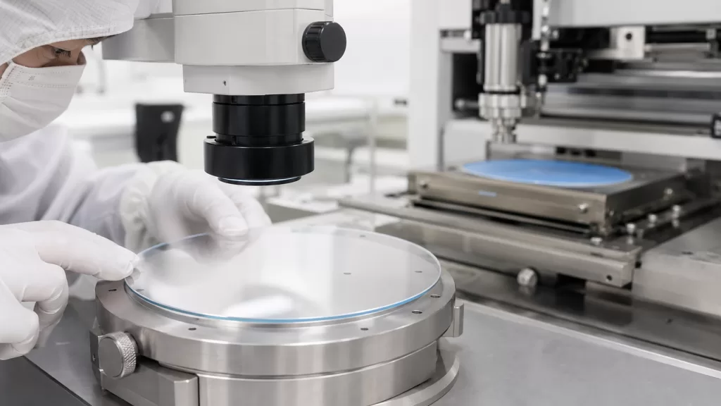
Edge defects can cause:
- Wafer breakage
- Particle generation
- Epitaxial cracking
- Reduced usable area
- Dicing-edge damage
- Equipment contamination
- Lower die yield
Two specifications are particularly important when purchasing sapphire substrates:
- Edge bevel or edge profile
- 에지 제외
These terms are related but not interchangeable. The bevel physically changes the wafer edge to reduce stress concentration. Edge exclusion defines a perimeter region that is excluded from inspection, patterning or usable-area calculations.
This guide explains how to specify both parameters and reduce sapphire chipping during epitaxy and dicing.
Why Sapphire Wafer Edges Are Vulnerable
Sapphire has high hardness and wear resistance, but hardness does not mean immunity to cracking.
During crystal processing, the wafer passes through:
- Boule orientation
- Wire sawing
- Edge grinding
- 랩핑
- 연마
- 청소
- Inspection
- Packaging
Each mechanical step can introduce small surface flaws or subsurface damage. A sharp or damaged edge concentrates stress into a small area.
Chipping may occur when the wafer experiences:
- Edge contact with a cassette
- Robot misalignment
- Vacuum chuck impact
- Local clamping force
- Thermal expansion during epitaxy
- Dicing-blade vibration
- Inadequate tape support
- High feed rate
- Incorrect cooling
- Poorly controlled entry or exit from a cut
A chip that appears cosmetic during incoming inspection may become the starting point of a larger crack after thermal cycling or dicing.
What Is a Sapphire Substrate Edge Bevel?
An edge bevel is a controlled removal of material from the sharp intersection between the front, backside and outer diameter of a wafer.
Instead of leaving a sharp 90-degree edge, the manufacturer creates a rounded or chamfered profile.
Common descriptions include:
- Rounded edge
- R-type edge
- Chamfered edge
- Double chamfer
- Beveled edge
- Custom edge radius
The correct profile depends on wafer diameter, thickness, orientation, handling equipment and downstream process.
Why Beveling Reduces Chipping
A sharp edge creates a strong local stress concentration. A properly manufactured bevel spreads mechanical stress over a larger region and removes unstable material left by slicing or edge grinding.
Benefits may include:
- Reduced edge-chipping risk
- Improved handling strength
- Lower wafer-breakage risk
- Smoother cassette loading
- Reduced particle generation
- Better resistance to thermal cycling
- More stable dicing entry and exit
- Improved edge inspection consistency
The bevel must also be smoothly polished. A poorly ground bevel containing deep scratches or microcracks may be more dangerous than a carefully prepared smaller bevel.
Edge Bevel Is Not the Same as an Optical Chamfer
Sapphire optical windows are sometimes specified with a simple chamfer such as a defined width at 45 degrees.
A semiconductor sapphire wafer may require a different edge profile because it must be compatible with:
- Wafer cassettes
- Robot end effectors
- Vacuum chucks
- Epitaxial susceptors
- Lithography equipment
- Dicing frames
Buyers should not copy an optical-window chamfer specification directly into a wafer RFQ without confirming equipment compatibility.
A wafer edge drawing is preferable when the edge profile is critical.
What Is Edge Exclusion?
Edge exclusion is a ring-shaped region extending inward from the physical outer edge of the wafer.
This area may be excluded from:
- Surface-defect acceptance
- Flatness calculations
- Film-uniformity calculations
- Lithography
- Device placement
- Die-yield calculations
- Electrical mapping
Edge exclusion is normally expressed as a radial distance in millimeters.
If a wafer has radius (R) and edge exclusion (E), the approximate effective radius becomes:
[
R_{\text{effective}} = R – E
]
The corresponding effective area is:
[
A_{\text{effective}} = \pi(R-E)^2
]
A larger exclusion zone provides more tolerance for edge roll-off and minor edge defects but reduces the available device area.
Edge Exclusion Does Not Physically Prevent Chipping
This distinction is important:
- Edge bevel helps reduce physical stress and chipping.
- Edge exclusion prevents the most vulnerable perimeter from being treated as fully usable device area.
Increasing edge exclusion does not repair a damaged wafer. It only prevents defects near the perimeter from being counted against central-area specifications or affecting the device layout.
A wafer with active cracks or unstable edge chips may still fail during epitaxy even if those defects are located outside the nominal usable area.
How the Edge Affects GaN-on-Sapphire Epitaxy
During GaN epitaxy, a sapphire wafer is exposed to high temperatures and significant thermal cycling.
GaN and sapphire have different lattice and thermal-expansion behavior. This produces stress in the epitaxial film and substrate during heating and cooling. Research on GaN layers grown on sapphire has documented thermally induced strain and wafer bending.
An existing edge chip can act as a stress concentrator when this thermal load is applied.
Potential consequences include:
- Crack propagation from the edge
- Local film delamination
- Wafer bow changes
- Particle release in the reactor
- Susceptor contamination
- Reduced edge-film uniformity
- Wafer breakage during cooling
Edge-Related Epitaxy Controls
To reduce risk before epitaxy:
- Use a smooth, consistent bevel
- Reject active cracks
- Define maximum acceptable edge-chip dimensions
- Inspect the complete circumference
- Remove polishing residue from the bevel
- Avoid edge contact during cleaning
- Match the edge profile to the susceptor
- Confirm backside cleanliness
- Use controlled heating and cooling ramps
- Prevent point loading at the wafer perimeter
The bevel should be completed before final cleaning and packaging.
How Edge Chipping Develops During Dicing
Sapphire dicing is a controlled brittle-material removal process. The cutting tool generates local mechanical stress that can create microfractures.
Chipping may appear on:
- Frontside cut edges
- Backside cut edges
- Blade entry points
- Blade exit points
- Corners of rectangular dies
- Intersections between dicing streets
- Areas containing pre-existing edge damage
Sapphire’s crystallographic orientation can influence crack propagation and dicing quality. Research on monocrystalline sapphire dicing found that cutting behavior changes with crystal direction and process configuration.
The dicing process should therefore be developed for the actual sapphire orientation, thickness and surface condition.
How to Reduce Sapphire Chipping During Blade Dicing
1. Select the Correct Diamond Blade
The blade should be selected according to:
- Sapphire thickness
- Required kerf width
- Die dimensions
- Frontside coating
- Backside condition
- Acceptable chip size
- Required throughput
Important blade characteristics include:
- Diamond grit size
- Diamond concentration
- Bond type
- Blade thickness
- Blade exposure
- Blade stiffness
A finer cutting system may reduce chipping but can also decrease throughput or increase blade loading. Qualification tests are required.
2. Control Feed Rate
A high feed rate increases the amount of material removed by each abrasive particle and can increase cutting force and chipping.
A systematic review of dicing-blade processes found that chipping generally increases with workpiece feed rate.
Start with conservative parameters and increase throughput only after edge quality is stable.
3. Optimize Spindle Speed
Increasing spindle speed may reduce chip load per abrasive particle, but only within the stable operating range of the blade and spindle.
Excessive speed, poor spindle condition or blade imbalance can create vibration and worsen the cut.
Spindle speed must be matched to:
- Blade diameter
- Bond type
- Grit size
- Blade exposure
- Cooling system
- Equipment condition
There is no universal spindle speed suitable for every sapphire wafer.
4. Use Stable Cooling and Debris Removal
Coolant helps:
- Remove heat
- Flush away sapphire debris
- Reduce blade loading
- Stabilize cutting conditions
- Protect surface coatings
Coolant nozzles should deliver stable flow to the cutting zone without lifting the wafer tape or creating uncontrolled vibration.
5. Verify Dicing Tape Support
Poor tape adhesion allows local wafer movement and increases backside chipping.
Check:
- Tape type
- Adhesion strength
- Frame tension
- Wafer mounting flatness
- Air bubbles
- Tape condition after cooling water exposure
Thin sapphire wafers may require additional carrier support.
6. Control Blade Entry and Exit
The start and end of a cut can experience unstable loading.
Possible improvements include:
- Extending the cutting street beyond the active area
- Using controlled entry speed
- Supporting the wafer edge
- Avoiding excessive blade exposure
- Applying a two-step or step-cut process
- Inspecting blade exit damage separately
7. Dress and Inspect the Blade
A glazed, loaded or unevenly worn blade can increase cutting force and lateral vibration.
Track:
- Blade wear
- Spindle current
- Cut count
- Dressing interval
- Kerf width
- Chipping trend
- Blade replacement history
8. Consider Laser or Stealth Dicing
Laser-based techniques may be considered when mechanical blade dicing produces unacceptable chipping or kerf loss.
Research has demonstrated near-infrared stealth dicing of sapphire by creating controlled internal modification zones before separation.
Laser processes still require optimization for:
- Sapphire thickness
- 오리엔테이션
- Focal depth
- Pulse energy
- Scan direction
- Coatings
- Separation force
Laser processing can introduce heat-affected regions, internal damage or debris if incorrectly configured.
Edge Defects That Should Be Included in Inspection
A complete edge inspection should distinguish between:
Edge Chip
A localized loss of material from the wafer edge.
Record:
- Width
- Depth
- Length
- Position
- Whether it reaches the main surface
Edge Crack
A fracture extending inward from the perimeter.
Cracks should normally be treated more seriously than isolated cosmetic chips because they can propagate during thermal cycling.
Bevel Scratch
A linear mark created during edge grinding, polishing, handling or cleaning.
Deep scratches may contain subsurface damage.
Edge Roll-Off
A gradual thickness or flatness change near the wafer perimeter caused by polishing.
Edge roll-off affects:
- Lithography focus
- Film uniformity
- Bonding
- Wafer geometry measurements
Bevel Contamination
Particles or residue trapped on the edge profile may detach during handling or epitaxy.
Wafer-edge engineering studies have shown that edge roughness, chipping and residues can generate particles or affect downstream process yield.
Recommended Edge Inspection Methods
Depending on the application, inspection may include:
- High-intensity light inspection
- Optical microscope inspection
- Automated edge inspection
- Dark-field inspection
- 360-degree bevel imaging
- Surface profilometry
- Confocal microscopy
- SEM analysis for failure investigation
The inspection report should state:
- Magnification
- Minimum detectable defect size
- Inspected edge region
- Edge-exclusion definition
- Number and maximum size of chips
- Crack acceptance criteria
- Whether the bevel and main surfaces were both inspected
Example Sapphire Substrate Edge Specification
The following example can be adjusted according to the process:
Material: Monocrystalline sapphire
지름: 100mm
오리엔테이션: C-플레인(0001)
Thickness: Buyer-defined nominal value and tolerance
Surface: SSP or DSP, epi-ready front surface
Edge Profile: Smooth rounded or double-chamfered wafer edge
Bevel Finish: Free from visible grinding cracks and unstable particles
Edge Exclusion: 3 mm radial example, subject to process confirmation
Edge Cracks: None permitted
Edge Chips: Maximum quantity and dimensions to be agreed
Main Surface Scratches: Defined within the usable area
TTV/Bow/Warp: Measured within the agreed exclusion zone
Inspection: Complete 360-degree edge inspection
포장: Individual cleanroom wafer container or compatible cassette
The 3 mm exclusion above is an example, not a universal sapphire standard. The final value should be coordinated with the epitaxy, lithography and dicing processes.
Sapphire Substrate RFQ Checklist
| RFQ Item | Information to Specify |
|---|---|
| 애플리케이션 | GaN epitaxy, LED, optical, MEMS or research |
| 지름 | 2, 4, 6 inch or custom |
| 두께 | Nominal value and tolerance |
| 오리엔테이션 | C-plane, A-plane, M-plane, R-plane or custom |
| Offcut | Angle, direction and tolerance |
| Surface | SSP or DSP |
| Front roughness | Maximum Ra or Sa |
| Backside finish | Ground, lapped or polished |
| Edge profile | Rounded, R-type, chamfer or custom drawing |
| Bevel dimensions | Radius, width, angle and tolerance |
| 에지 제외 | Radial distance from physical edge |
| Edge cracks | Acceptance criteria |
| Edge chips | Quantity and maximum dimensions |
| Edge scratches | Acceptance criteria |
| Edge roll-off | Measurement and limit if critical |
| TTV/Bow/Warp | Limits and measurement exclusion |
| Flat or notch | Dimensions and orientation |
| Dicing method | Blade, laser or customer-developed |
| Inspection | Optical, automated bevel scan or microscopy |
| Packaging | Single-wafer box or cassette |
| Quantity | Samples, qualification or production volume |
Common Purchasing Mistakes
Specifying Only “Beveled Edge”
This does not define the edge radius, chamfer width, angle, finish or tolerance.
Assuming Edge Exclusion Removes Breakage Risk
An excluded crack can still propagate and break the wafer.
Using an Optical-Window Chamfer for a Wafer
Optical windows and semiconductor wafers may require different edge profiles and handling compatibility.
Ignoring Flat and Notch Transitions
The ends of a primary flat or the geometry around a notch can become stress-concentration areas. These regions should also be inspected.
Accepting Only Frontside Inspection
Backside edge chips can grow during dicing or thermal cycling. Both sides and the complete bevel should be inspected.
Using Generic Dicing Parameters
Sapphire diameter, thickness, orientation, coating and die geometry can all change the optimum dicing conditions.
Frequently Asked Questions
What is the difference between edge bevel and edge exclusion?
The bevel is the physical shape of the wafer edge. Edge exclusion is the perimeter region omitted from usable-area or inspection calculations.
Does a larger bevel always reduce chipping?
No. An excessively large or poorly polished bevel may reduce usable area or create handling incompatibility. The profile must match the wafer thickness and equipment.
What edge exclusion should be used for a sapphire wafer?
There is no universal value. It should be defined according to wafer diameter, bevel geometry, epitaxy uniformity, lithography and dicing layout.
Can a chipped sapphire wafer still be used for epitaxy?
A small stable chip outside the usable area may be acceptable in some research processes. Active cracks, deep chips or loose particles create much greater risk and should normally be rejected.
Is blade dicing or laser dicing better for sapphire?
Both can work. Blade dicing is established and economical, while laser or stealth dicing may reduce kerf or mechanical force. The best method depends on thickness, coating, orientation, die size and acceptable damage.
Should dicing direction follow the sapphire crystal orientation?
Crystal direction can influence crack behavior and cut quality. The dicing process should be qualified for the specific wafer orientation and die layout.
When should the edge bevel be produced?
The bevel should normally be completed during substrate manufacturing before final polishing, cleaning and packaging.
결론
Sapphire wafer chipping cannot be controlled by a single specification.
A reliable edge-management strategy combines:
- A properly designed and polished edge bevel
- A clearly defined edge-exclusion region
- Complete 360-degree edge inspection
- Controlled cleanroom handling
- Compatible epitaxy carriers
- Stable thermal ramps
- Qualified dicing blades or laser parameters
- Strong wafer and tape support
The bevel reduces physical stress concentration. Edge exclusion protects the device design and inspection plan from the least stable perimeter region. Neither one can compensate for active cracks, poor polishing or an uncontrolled dicing process.
Before requesting a quotation, buyers should provide the sapphire orientation, diameter, thickness, surface finish, edge-profile drawing, exclusion distance, maximum chip size, crack criteria and downstream process.
A complete edge specification helps reduce wafer breakage, reactor particles, dicing damage and avoidable device-yield loss.