
In modern power electronics, Silicon Carbide has become one of the most important wide-bandgap semiconductor materials. Compared with traditional Silicon, SiC offers superior properties such as higher breakdown electric field, better thermal conductivity, and the ability to operate at higher temperatures and voltages. Because of these advantages, SiC is widely used in power devices for electric vehicles, renewable energy systems, and high-frequency power converters.
Among the various polytypes of SiC, 4H‑SiC is currently the most widely used for power semiconductor substrates. During wafer manufacturing, polishing, and epitaxial growth, two crystallographic surfaces are frequently mentioned: the carbon face (C-face) and the silicon face (Si-face). Understanding the difference between these two surfaces is important for both material processing and device fabrication.
1. Crystal Structure of Silicon Carbide
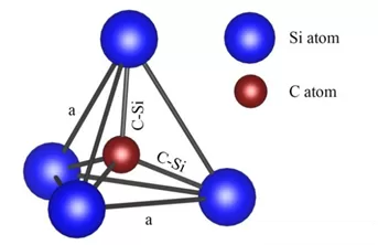
Silicon carbide is a covalently bonded crystal composed of silicon and carbon atoms arranged in a tetrahedral coordination structure. Each silicon atom is bonded to four carbon atoms, and each carbon atom is bonded to four silicon atoms, forming a strong three-dimensional lattice.
SiC exists in many different crystal polytypes, mainly divided into two structural families:
- Cubic structure (β-SiC) – also known as the zinc-blende structure
- Hexagonal structure (α-SiC) – including polytypes such as 4H-SiC and 6H-SiC
In hexagonal SiC crystals, the atomic layers stack along the C축 of the crystal. When a wafer is sliced from the crystal boule along this axis, two opposite polar surfaces appear. These two surfaces correspond to the silicon-terminated surface and the carbon-terminated surface, which are commonly called the Si-face and C-face.
2. What Is the Silicon Face (Si-Face)?
그리고 silicon face, also known as the (0001) plane, is the crystal surface obtained when the wafer is cut along the positive direction of the c-axis. On this surface, the outermost atomic layer is terminated by silicon atoms.
The Si-face is particularly important in semiconductor manufacturing because it offers more stable and controllable conditions for epitaxial growth. As a result, most commercial SiC power device wafers are processed with the Si-face as the device side.
Key characteristics of the Si-face include:
- More stable surface reconstruction
- Better control of epitaxial growth processes
- Higher interface quality with dielectric materials
- More mature industrial processing technology
Because of these advantages, the Si-face is the dominant orientation used in SiC MOSFET and Schottky diode manufacturing.
3. What Is the Carbon Face (C-Face)?
그리고 carbon face, also called the (000-1) plane, is the surface obtained when the crystal is cut along the negative direction of the c-axis. In this orientation, the outermost atoms exposed on the surface are carbon atoms.
Although less commonly used for device fabrication, the C-face has unique properties that make it useful in certain processes.
Typical characteristics of the C-face include:
- Faster epitaxial growth rates
- Different surface chemistry compared with the Si-face
- Higher tendency for step bunching during growth
- Distinct oxidation and interface behavior
In some crystal growth processes, particularly during SiC bulk crystal growth, the C-face may be used as the seed growth surface.
4. Why the Difference Matters in Manufacturing
Although both faces belong to the same crystal and therefore have the same bulk hardness and mechanical properties, their surface atomic termination leads to different chemical and electronic behaviors.
These differences affect several key processes in semiconductor manufacturing:
- Epitaxial Growth
The Si-face generally produces smoother and more controllable epitaxial layers. - Oxide Interface Quality
Device structures such as MOSFETs require high-quality oxide interfaces, which are typically better achieved on the Si-face. - Surface Processing and Polishing
Surface reactions during polishing, etching, and cleaning can differ between the two faces. - Device Reliability
The orientation used can influence interface trap density and electrical performance.
For these reasons, most commercial SiC wafers are designed with the Si-face as the functional device surface.
5. How to Identify the C-Face and Si-Face
In industrial wafer production, manufacturers typically mark wafer orientation using flats, notches, or V-groove indicators on the wafer edge. These markers help identify the crystal orientation and determine which side is the Si-face.
In research laboratories, several advanced techniques may also be used to distinguish the two surfaces, including:
- Surface potential measurements using scanning probe methods
- Surface energy testing using wetting liquids
- Surface spectroscopy analysis
These methods allow researchers to identify the two faces without damaging the wafer.
결론
The carbon face (C-face) and silicon face (Si-face) of a SiC wafer refer to two opposite crystallographic surfaces determined by the orientation of the crystal along the c-axis. Although they belong to the same material and share identical bulk mechanical properties, their different atomic terminations result in distinct surface chemistry and processing behavior.
Because the Si-face provides better epitaxial growth quality and interface characteristics, it has become the standard surface used in most commercial SiC power device manufacturing. Understanding the differences between these two surfaces is therefore essential for wafer processing, epitaxy, and semiconductor device fabrication.