
Silicon carbide (SiC) has transformed the landscape of power electronics. From electric vehicle (EV) inverters to high-frequency converters, SiC enables devices to operate faster, hotter, and more efficiently than traditional silicon. Yet, not all SiC substrates are created equal. Choosing the right one is a strategic decision that directly affects device performance, yield, and reliability.
This article explores the key factors you must consider when selecting a SiC substrate, breaking down complex materials science into practical guidance for engineers, researchers, and tech enthusiasts.
1. Polytype Matters: 4H-SiC vs 6H-SiC
SiC is polymorphic—it exists in multiple crystal structures called polytypes, each with unique electrical and thermal properties.
- 4H-SiC: The preferred choice for high-voltage and high-speed devices. Its wide bandgap (~3.26 eV) and high electron mobility (~1000 cm²/V·s) make it ideal for MOSFETs, Schottky diodes, and EV inverters.
- 6H-SiC: With a slightly narrower bandgap (~3.02 eV) and lower electron mobility (~450 cm²/V·s), it is better suited for RF devices or low-power high-voltage applications.
Tip: If your project demands fast switching and low leakage current under high voltage, 4H-SiC is non-negotiable.
2. Doping Type: N-type, P-type, or Semi-Insulating?
SiC substrates are available in different doping types, which determine how they conduct electricity:
- N-type: Electron-dominant conduction, commonly used in MOSFETs and Schottky diodes.
- P-type: Hole-dominant conduction, used in complementary devices and certain diode structures.
- Semi-Insulating (SI): Electrically neutral, ideal for RF devices and devices requiring minimal parasitic conduction.
Insight: Selecting the wrong doping type is like choosing the wrong foundation for a building—it compromises efficiency and reliability.
3. Crystal Quality: Defects Are Hidden Killers
High-quality crystal structure is the backbone of high-performance devices. Key factors include:
- Gęstość mikrorurek: Fewer micropipes mean fewer short circuits.
- Gęstość dyslokacji: High dislocation levels reduce yield and reliability.
- Resistivity uniformity: Ensures consistent device performance across the wafer.
Even minor defects at the atomic level can cause significant problems in high-power applications, so demand detailed crystal quality reports from suppliers.
4. Wafer Size and Thickness: Handling vs Throughput
Larger wafers increase manufacturing throughput but are more difficult to handle and more prone to breakage. Thickness affects:
- Thermal management: Thinner wafers improve heat dissipation but are fragile.
- Mechanical stability: Thicker wafers are easier to handle but may require advanced cooling in high-power applications.
Practical advice: Balance wafer size with your equipment capabilities and risk tolerance. For industrial EV modules, 6–8 inch wafers are standard; for lab-scale research, 4-inch wafers suffice.
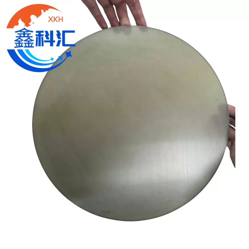
5. Surface Finish: Polishing Makes a Difference
Surface roughness may seem minor, but in semiconductor fabrication, it determines:
- Epitaxial layer uniformity
- Lithography precision
- Etching and dicing quality
Pro tip: Opt for wafers with chemical mechanical polishing (CMP). While slightly more expensive upfront, CMP wafers reduce defects, improve yield, and save costs downstream.
6. Thermal and Mechanical Robustness
SiC’s high thermal conductivity is one of its biggest advantages, but each wafer has mechanical limits. Thermal cycling or high current densities can cause cracks or warping. Evaluate:
- Thermal conductivity (≥3.5 W/cm·K for power devices)
- Coefficient of thermal expansion, compatible with epitaxial layers
- Flexural strength to ensure mechanical robustness during handling
7. Supplier Reliability: Consistency Counts
Bulk purchasing amplifies risk. Even minor inconsistencies in crystal quality or wafer handling can lead to massive losses. Look for suppliers who provide:
- Lot-to-lot uniformity
- Traceable quality reports
- Proven experience in power electronics-grade wafers
Red flag: If a supplier cannot provide detailed defect densities, resistivity mapping, and surface roughness measurements, reconsider your order.
8. Application Alignment: Know Your Device Requirements
Ultimately, the right substrate depends on device and application requirements:
- High-voltage MOSFETs, inverters → 4H-SiC, N-type or SI
- Schottky diodes → 4H-SiC, N-type
- RF devices, microwave components → 6H-SiC, SI
- LEDs and optoelectronic devices → Either 4H or 6H depending on growth conditions
Rule of thumb: Device performance is only as good as the substrate underneath it.
Final Thoughts
Choosing a SiC substrate is more than just a materials selection exercise—it’s a strategic engineering decision that affects yield, efficiency, and long-term reliability. By carefully evaluating:
- Polytype (4H vs 6H)
- Doping type (N, P, SI)
- Crystal quality
- Wafer size and thickness
- Surface finish
- Thermal and mechanical robustness
- Supplier reliability
- Application alignment
…you can ensure your power electronics devices achieve their full potential.
Remember: In power electronics, the right substrate isn’t just a foundation—it’s the difference between a high-efficiency device and a production nightmare.