
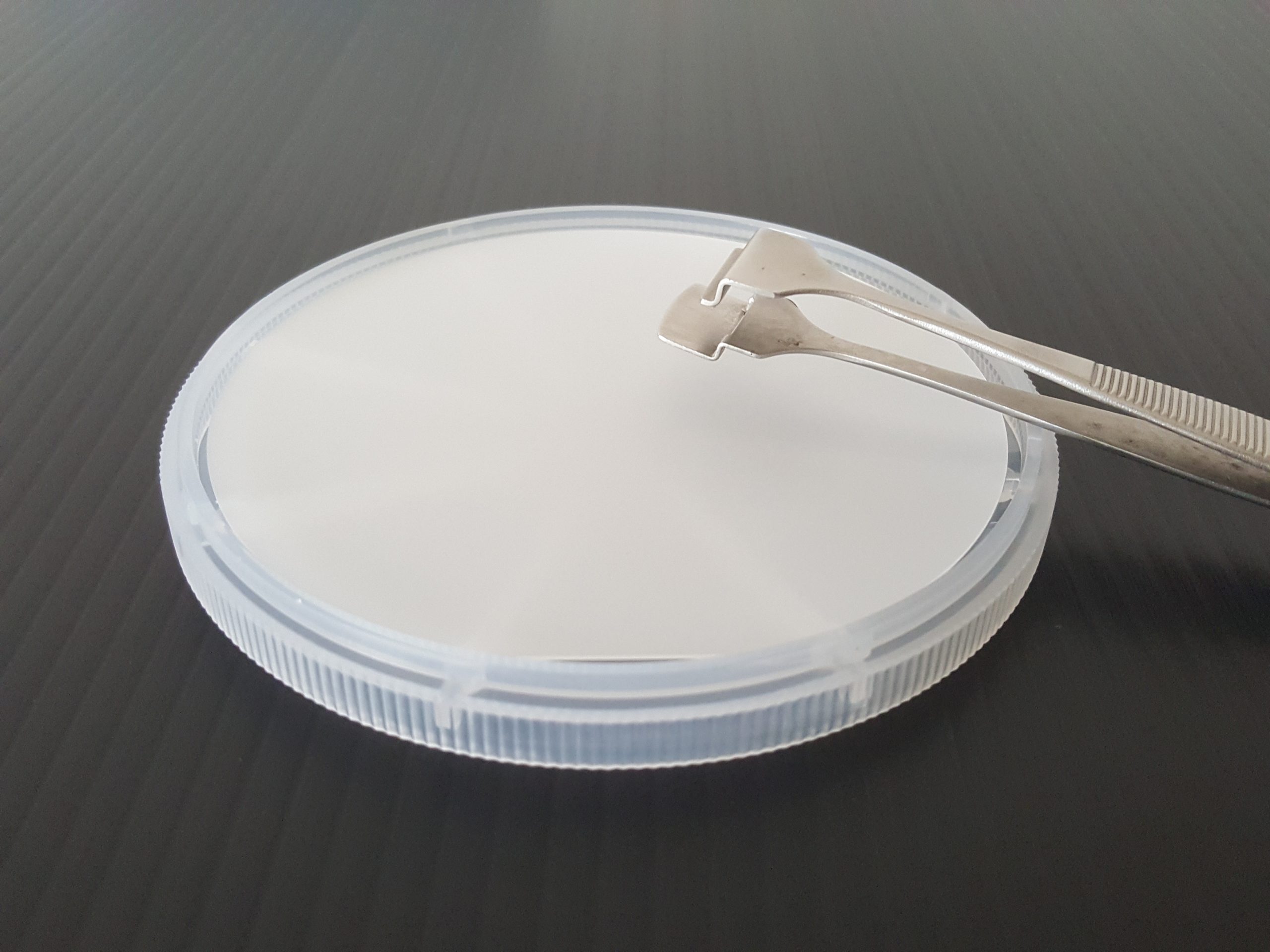
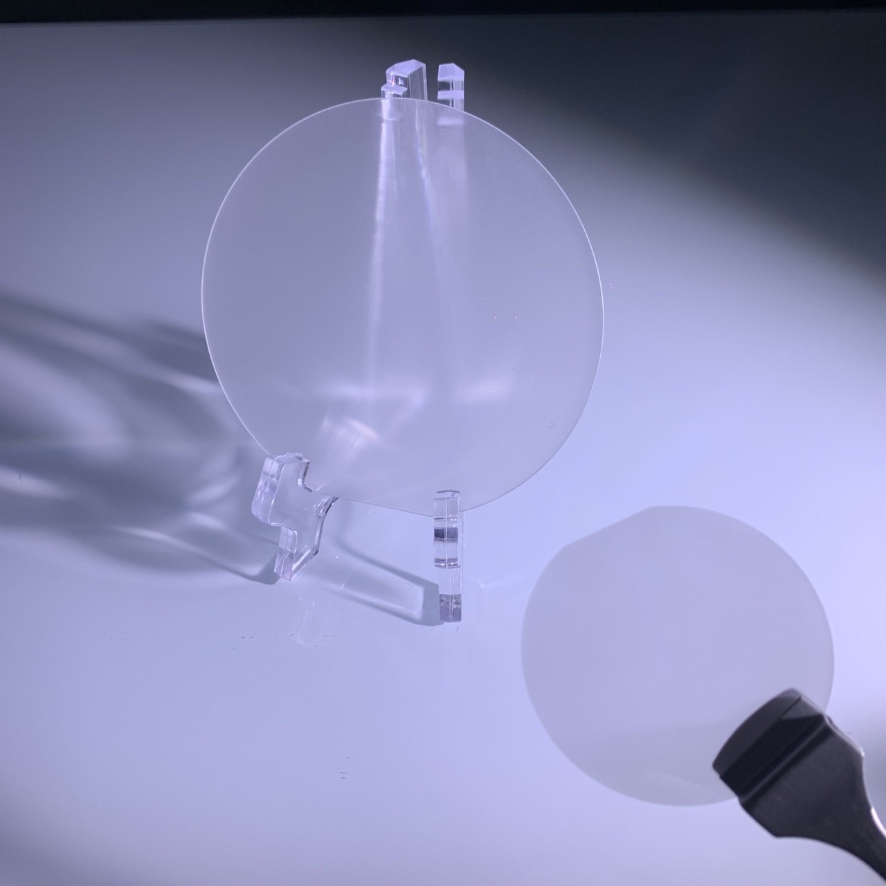
Podłoża szafirowe, powszechnie nazywane waflami szafirowymi, to najnowocześniejsze materiały o szerokim spektrum zastosowań w różnych branżach. Wykonane z krystalicznego tlenku glinu wafle szafirowe są cenione za wyjątkową twardość, przezroczystość optyczną i trwałość termiczną. W tym podsumowaniu produktu omówione zostaną kluczowe atrybuty i zastosowania produktów szafirowych.
Cechy szafirowego podłoża/wafla
część 1
- Twardość: Wyjątkowa twardość, ustępująca jedynie diamentom.
- Przejrzystość: Wysoka przezroczystość optyczna w szerokim spektrum.
- Przewodność cieplna: Wysoka przewodność cieplna zapewnia efektywne odprowadzanie ciepła.
- Odporność na szok termiczny: Odporny na szok termiczny, zachowujący stabilność w zmiennych temperaturach.
- Wymiary konfigurowalne: Dostępne w konfigurowalnych rozmiarach i grubościach do różnych zastosowań.
- Struktura kryształu: Skład monokrystalicznego tlenku aluminium.
- Odporność chemiczna: Odporność na wiele chemikaliów, zwiększająca trwałość.
- Wykończenie powierzchni: Możliwość uzyskania gładkiego i wypolerowanego wykończenia powierzchni.
część 2
- Transmisja długości fali: Efektywna transmisja różnych długości fal, szczególnie w zakresie widzialnym i bliskiej podczerwieni.
- Izolacja elektryczna: Doskonałe właściwości izolacji elektrycznej.
- Wszechstronność: Nadaje się do szerokiego zakresu zastosowań w elektronice, optyce i półprzewodnikach.
- Długowieczność: Wysoka odporność na zarysowania i zużycie zapewnia długą żywotność.
- Przejrzystość optyczna: Zapewnia wyraźną jakość optyczną obrazowania i komponentów optycznych.
- Możliwość produkcji: Kompatybilność z różnymi procesami produkcyjnymi.
- Personalizacja: Możliwość dostosowania do konkretnych wymagań branżowych i aplikacji.
- Niezawodność: Znany z niezawodności i wydajności w wymagających środowiskach.
Szafirowe wafle wykazują unikalne cechy, które czynią je wysoce pożądanymi w różnych branżach. Po pierwsze, są one znane ze swojej wyjątkowej twardości i odporności na zarysowania. Co więcej, ich wysoka temperatura topnienia i przewodność cieplna przyczyniają się do ich przydatności w wymagających zastosowaniach.
Oprócz właściwości mechanicznych, płytki szafirowe charakteryzują się doskonałą przezroczystością optyczną w szerokim spektrum, od ultrafioletu do podczerwieni. Ta cecha czyni je idealnymi do urządzeń optoelektronicznych, takich jak diody LED i diody laserowe. Co więcej, struktura krystaliczna szafiru zapewnia jednorodność, zapewniając spójne podłoże do zastosowań elektronicznych i fotonicznych.
Z drugiej strony wyróżniają się one obojętnością chemiczną, dzięki czemu są odporne na działanie środowisk korozyjnych. Właściwość ta jest korzystna w zastosowaniach, w których narażenie na działanie agresywnych chemikaliów jest problemem. Niemniej jednak, pomimo swojej wytrzymałości, szafirowe płytki podłoża są stosunkowo lekkie, co przyczynia się do ich atrakcyjności w przemyśle lotniczym i przenośnych urządzeniach elektronicznych.
W przeciwieństwie do tradycyjnych płytek krzemowych, podłoża szafirowe oferują lepszą izolację elektryczną. Jest to kluczowa cecha w produkcji elektroniki mocy, gdzie minimalizacja strat elektrycznych jest najważniejsza. Podobnie, wysoka wytrzymałość dielektryczna szafiru zwiększa jego wydajność w zastosowaniach o wysokiej częstotliwości i dużej mocy.
Ponadto wykazuje niski współczynnik rozszerzalności cieplnej, zmniejszając prawdopodobieństwo pękania lub wypaczania pod wpływem zmian temperatury. Cecha ta jest szczególnie korzystna w sytuacjach, w których niezbędna jest stabilność termiczna, np. w procesach produkcji półprzewodników.
Wszechstronność szafiru jako materiału podłoża jest dodatkowo potwierdzona przez jego kompatybilność z różnymi technikami osadzania. Obejmuje to fizyczne osadzanie z fazy gazowej (PVD), chemiczne osadzanie z fazy gazowej (CVD) i epitaksjalne metody wzrostu. W związku z tym producenci mają swobodę wyboru najbardziej odpowiedniej techniki dla swoich konkretnych zastosowań.
Podsumowując, kompleksowy zestaw cech, obejmujący wytrzymałość mechaniczną, przezroczystość optyczną, odporność chemiczną, izolację elektryczną i stabilność termiczną, pozycjonuje go jako materiał z wyboru w różnych gałęziach przemysłu. Płynna integracja tych cech, w połączeniu z ciągłym postępem w technologiach produkcji, gwarantuje, że szafirowe wafle substratowe będą nadal odgrywać kluczową rolę w rozwoju innowacji technologicznych w wielu sektorach.
Sapphire Substrate/wafer‘s Application
- Semiconductor Fabrication: Used as substrates for manufacturing semiconductor devices and integrated circuits.
- LEDs (Light Emitting Diodes): Employed in the production of high-performance LEDs for lighting applications.
- Optical Windows: Utilized as transparent windows in optical systems, cameras, and sensors.
- Laser Diodes: Substrates for laser diodes due to their optical clarity and thermal properties.
- Elektronika mocy: Applied in power electronic devices for efficient heat dissipation.
- Watch Crystals: Used as watch crystals due to their hardness and scratch resistance.
- Aerospace Components: Found in aerospace applications for their durability and reliability.
- Urządzenia medyczne: Used in medical equipment where optical clarity and biocompatibility are crucial.
- High-Performance Electronics: Employed in high-performance electronic components.
- RF (Radio Frequency) Applications: Used in RF devices and components.

- Infrared (IR) Windows: Applied in IR systems for their transparency in the infrared spectrum.
- Optical Lenses: Utilized in the production of optical lenses for various imaging systems.
- Transparent Armor: Used in military applications as transparent armor due to its hardness.
- Czujniki: Incorporated in sensors for their optical and thermal properties.
- Thin-Film Coatings: Used as a substrate for thin-film coatings in various applications.
- Biomedical Devices: Applied in biomedical devices for their biocompatibility.
- MEMS (Micro-Electro-Mechanical Systems): Used as substrates in MEMS devices.
- Telecommunications: Employed in telecommunications devices and components.
- Photovoltaic Devices: Used in the production of high-efficiency photovoltaic cells.
- Consumer Electronics: Found in various consumer electronics for display and sensor applications.
Sapphire Substrate/wafer Available Dimensions
| Standard wafer(customzied)2 inch C-plane sapphire wafer SSP/DSP 3 inch C-plane wafer SSP/DSP 4 inch C-plane wafer SSP/DSP 6 inch C-plane wafer SSP/DSP8 inch C-plane wafer SSP/DSP12 inch C-plane wafer SSP/DSP | Special Cut A-plane (1120) wafer 430um/500um R-plane (1102) wafer 430um/500um M-plane (1010) wafer 430um/500um N-plane (1123) wafer 430um/500um C-axis with a 0.5°~ 4° offcut, toward A-axis or M-axis Other customized orientation |
| Customized Size 10*10mm sapphire wafer 20*20mm sapphire wafer Ultra thin (100um) sapphire wafer 8 inch sapphire wafer | Patterned Sapphire Substrate (PSS) 2 inch C-plane PSS 4 inch C-plane PSS |
| 2inch wafers in stock | DSP C-AXIS 0.1mm/0.175mm/0.2mm/0.3mm/0.4mm/0.5mm/ 1.0mmtSSP C-axis 0.2/0.43mm(DSP&SSP) A-axis/M-axis/R-axis 0.43mm |
| 3inch in stocks; | DSP/ SSP C-axis 0.43mm/0.5mm |
| 4Inch in stocks | C-planedsp c-axis 0.4mm/ 0.5mm/1.0mmssp c-axis 0.5mm/0.65mm/1.0mmt |
| 6inch wafers in stocks | C-planessp c-axis 1.0mm/1.3mmm dsp c-axis 0.65mm/ 0.8mm/1.0mmt |
| 8 inch sapphire wafers in stock | C-planessp c-axis 1.15mm/1.6mmm DSP c-axis 0.725mm/ 1.6mm/1.8mmt |
12inch Wafers in stocks | C-plane DSP c-axis 0.725mm/ 1.5mm/1.0mmt |
Sapphire Substrate/wafer Q&A
Q:Why sapphire is used as substrate?
A:Sapphire substrates. Sapphire (β-Al2O3) is the most popular and extensively used substrate for the growth of III-nitride. It is optically transparent from the visible into deep UV. Similarly It is stable at high temperatures and pre-growth cleaning is well established due to its use in SOI wafer fabrication in Si technology.
Q:What is the chemical composition of the sapphire substrate?
A:Sapphire is a crystalline form of aluminum oxide (Al2O3). It is formed of Al3+ cations and O2- anions arranged in a hexagonal lattice. It is extremely unreactive and chemically-resistant to acids and alkalis, including hydrofluoric acid.
Q:What is sapphire wafer?
Sapphire Wafers. Product Description: Sapphire is a material of a unique combination of physical, chemical and optical properties, which make it resistant to high temperature, thermal shock, water and sand erosion, and scratching. It is a superior window material for many IR applications from 3µm to 5µm.
Sapphire Substrate/wafer Simple Processing Procedure
Sapphire Wafer Production Methods:
In particular they are commonly produced using the following methods:
Kyropoulos Method:
This method involves crystallizing sapphire from a molten alumina source.
A seed crystal is dipped into the molten alumina and slowly pulled upward to form a single crystal.
Heat Exchanger Method:
In fact in this method, a mixture of alumina powder and a seed crystal is placed in a crucible.
The crucible is heated through a heat exchanger, causing the alumina to melt and crystallize onto the seed.
Edge-Defined Film-Fed Growth (EFG) Method:
EFG involves drawing a ribbon of alumina through a heated zone where it crystallizes into a sapphire film.
This method allows for continuous production of them.
Czochralski (CZ) Method:
The CZ method involves melting alumina in a crucible and slowly pulling a seed crystal from the melt.
The pulled crystal is then sliced into wafers.
Liquid Phase Epitaxy (LPE):
Likewise LPE involves the deposition of sapphire onto a substrate from a supersaturated solution.
The product is immersed in the solution, and the sapphire layer grows on its surface.
Plasma-Assisted Reactive Magnetron Sputtering:
This is a thin film deposition technique where it is deposited onto a using plasma and magnetron sputtering.
Wafering:
Meanwhile After the crystal growth, the sapphire ingot is sliced into thin wafers using techniques like diamond wire sawing or laser cutting.
Polishing:
To sum up the sliced wafers undergo a polishing process to achieve the desired surface smoothness and thickness uniformity.
Its significance
The sapphire wafer plays a pivotal role in the semiconductor industry, contributing significantly to various technological advancements and applications. Its unique properties make it a preferred substrate for a wide range of electronic and optoelectronic devices. In this comprehensive exploration, we delve into the crucial role that sapphire wafers play in the semiconductor landscape.
Crystal Clarity and Structural Uniformity: One of the key attributes of sapphire wafers is their crystal clarity and structural uniformity. The crystalline nature of sapphire ensures a consistent and well-defined lattice structure, providing an excellent foundation for semiconductor device fabrication. This structural uniformity is crucial for achieving precision in the manufacturing process.
Optical Transparency Across the Spectrum: Sapphire wafers exhibit exceptional optical transparency across a broad spectrum, from ultraviolet to infrared wavelengths. This unique property makes them ideal for optoelectronic applications, including light-emitting diodes (LEDs) and laser diodes. The optical clarity of sapphire enhances the performance of these devices, contributing to the efficiency and reliability of optical communication systems.
Mechanical Hardness and Durability: The remarkable hardness of sapphire, second only to diamond, makes it highly resistant to scratches and wear. This mechanical durability is a significant advantage in semiconductor manufacturing, where delicate processes and precision are paramount. Sapphire wafers provide a robust substrate that withstands the challenges of fabrication and handling, ensuring the integrity of the final semiconductor devices.
Thermal Stability and Heat Dissipation: Sapphire wafers possess excellent thermal stability and high thermal conductivity. This makes them well-suited for applications that involve high temperatures or require efficient heat dissipation. In semiconductor devices that generate heat during operation, such as power electronics and high-frequency components, sapphire wafers play a crucial role in maintaining thermal stability and preventing overheating.
Electrical Insulation Properties: In contrast to traditional silicon wafers, sapphire wafers offer superior electrical insulation. This property is particularly valuable in power electronics, where minimizing electrical losses is essential. The electrical insulation provided by sapphire substrates contributes to the efficiency of electronic components and enables the development of high-performance semiconductor devices.
Chemical Inertness and Corrosion Resistance: Sapphire is known for its chemical inertness and resistance to corrosion. This characteristic makes sapphire wafers suitable for environments where exposure to harsh chemicals is a concern. In semiconductor manufacturing, where various chemicals are used in processing, the chemical resistance of sapphire ensures the longevity and reliability of the semiconductor devices.
Versatility in Deposition Techniques: Sapphire wafers exhibit versatility in terms of compatibility with different deposition techniques. Whether it’s physical vapor deposition (PVD), chemical vapor deposition (CVD), or epitaxial growth methods, sapphire provides a versatile substrate for diverse manufacturing processes. This flexibility allows semiconductor manufacturers to choose the most appropriate deposition technique for their specific applications.
Applications in Emerging Technologies: The significance of sapphire wafers extends to emerging technologies such as gallium nitride (GaN) devices. GaN-based semiconductors, used in power electronics and high-frequency applications, often leverage sapphire wafers as the substrate of choice. This underscores the role of sapphire in fostering innovation and progress in cutting-edge semiconductor technologies.
Wnioski: In conclusion, the sapphire wafer stands as a cornerstone in the semiconductor industry, contributing to advancements in electronic and optoelectronic technologies. Its crystal clarity, optical transparency, mechanical hardness, thermal stability, electrical insulation, chemical inertness, and versatility in manufacturing processes make it a preferred substrate for a diverse range of semiconductor applications. As technology continues to evolve, the role of sapphire wafers is likely to expand, driving innovation and enabling the development of more advanced and efficient semiconductor devices.