
Description
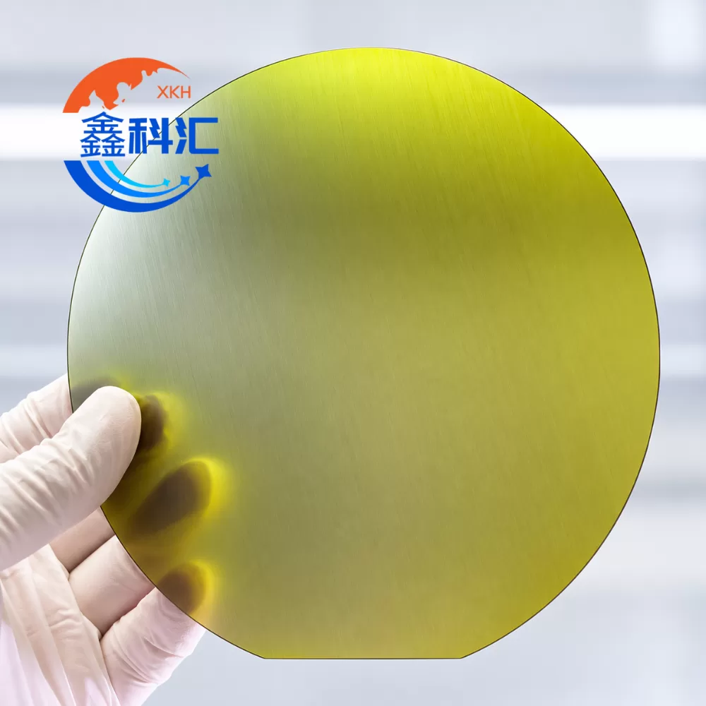
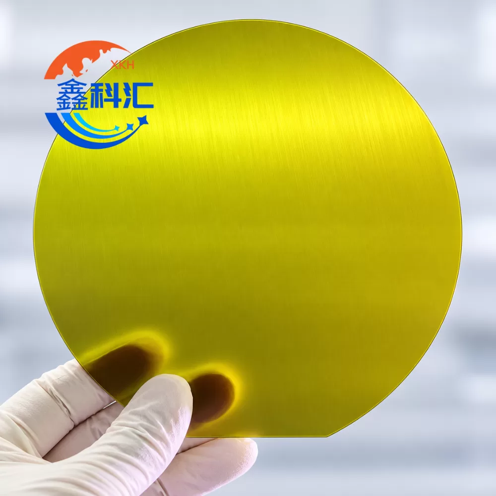
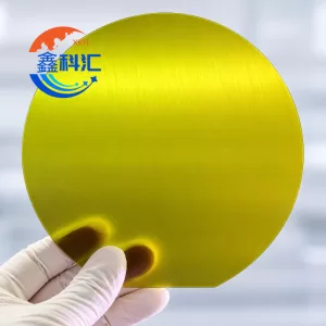
The 6 Inch SiC As-Cut Wafer is a silicon carbide wafer supplied directly after slicing from a SiC crystal boule, before final grinding, lapping, polishing, or CMP treatment.
This product is intended for customers who require genuine SiC wafer material for downstream processing, machining trials, polishing development, equipment qualification, or semiconductor process evaluation, without the additional cost of a fully polished substrate.
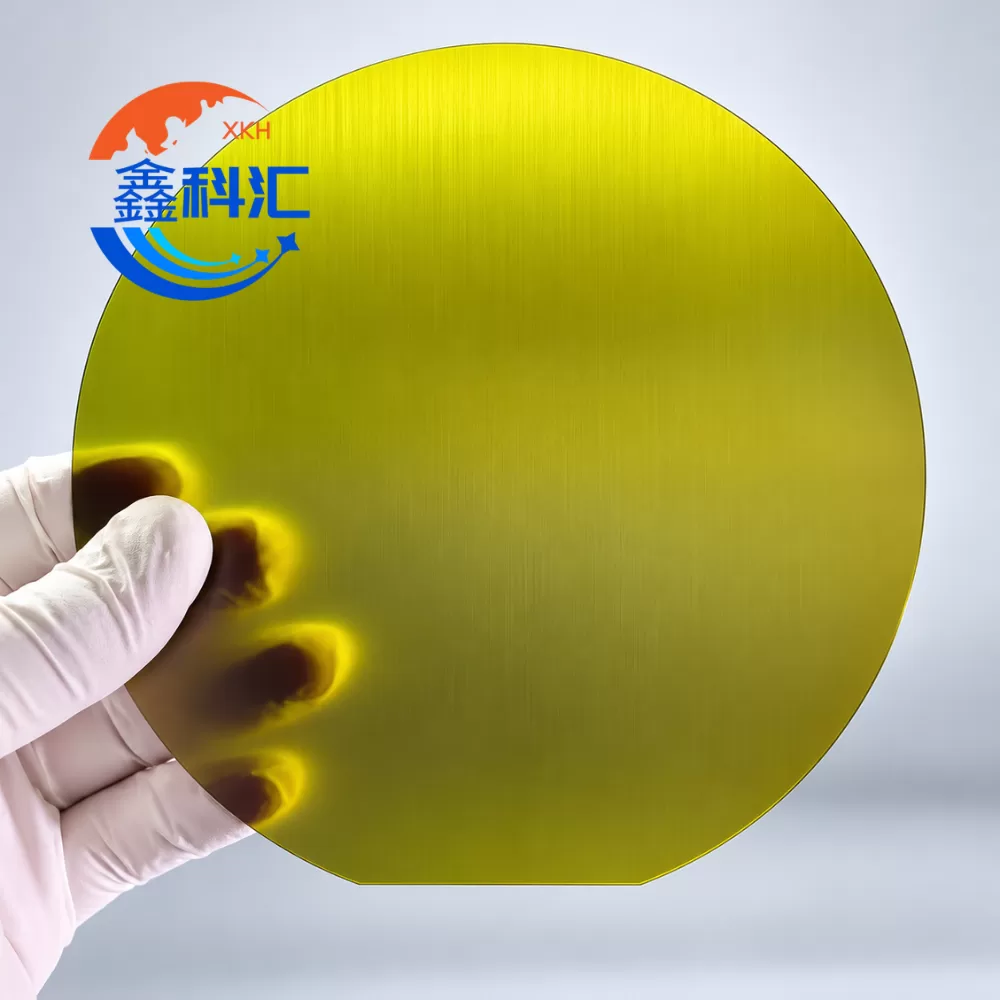
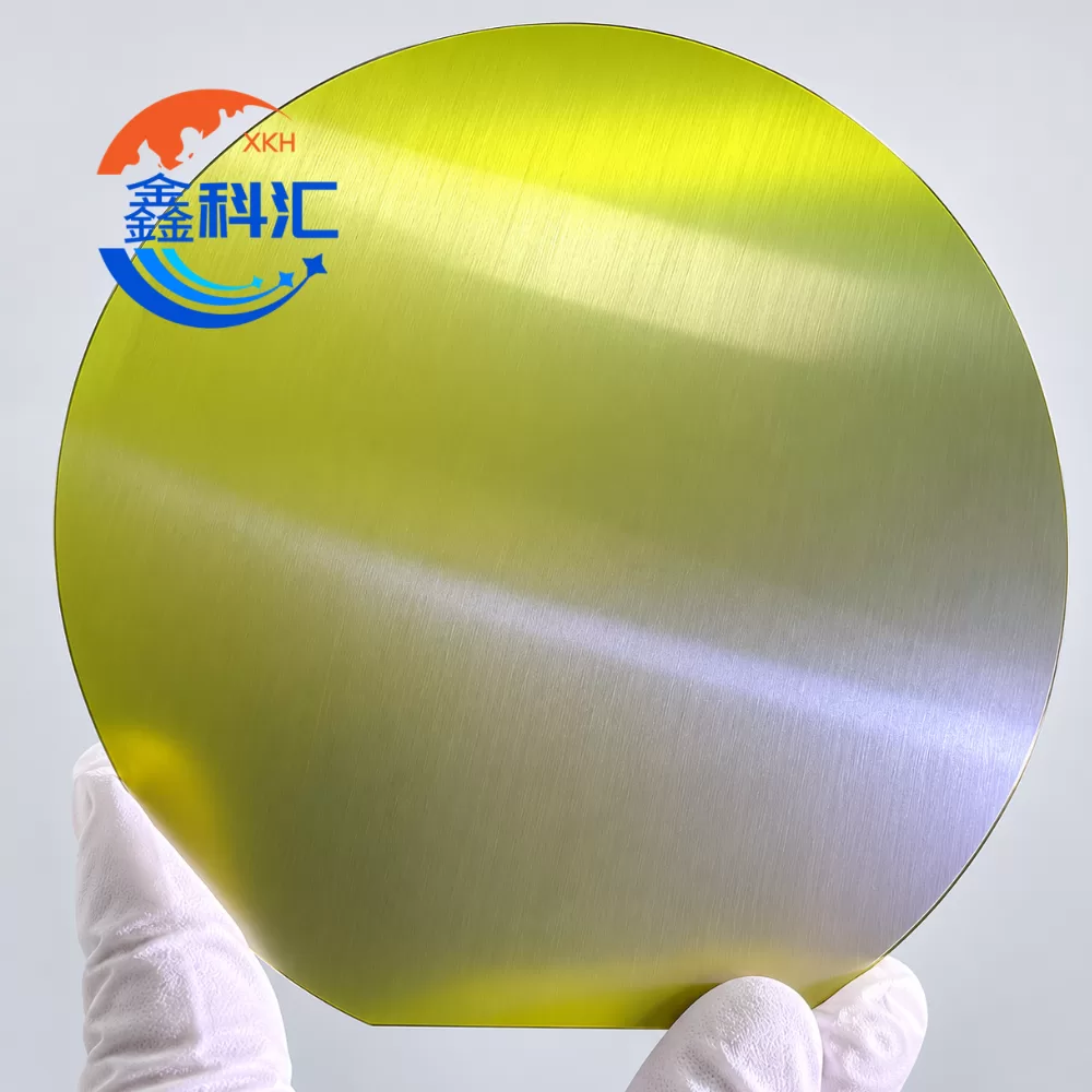
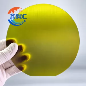
The wafer retains its original as-sliced surface and may show visible cutting lines or machining traces. These features are normal for an as-cut wafer and make the product suitable for further processing.
Customized thickness, crystal type, conductivity, orientation, and edge configuration are available according to project requirements.
 Key Advantages
 Key Advantages
- 6 inch / 150 mm silicon carbide wafer
- Supplied in as-cut condition
- No final polishing or CMP
- Suitable for grinding and lapping
- Suitable for polishing process development
- Ideal for semiconductor equipment testing
- Cost-effective for R&D and process trials
- Custom thickness and material specifications available
- Suitable for sample orders and batch supply
General Specifications
| Item | Specification |
|---|---|
| Material | Silicon Carbide (SiC) |
| Diameter | 6 Inch / 150 mm |
| Wafer Type | As-Cut / As-Sliced |
| Surface Condition | Unpolished |
| Polytype | 4H-SiC / 6H-SiC / Custom |
| Conductivity | N-Type / Semi-Insulating / Custom |
| Orientation | Standard or Customized |
| Thickness | Customizable |
| Edge Type | Flat / Notch / Customized |
| Processing Status | Before Final Grinding and Polishing |
| Order Quantity | Samples, Small Batches, Volume Orders |
Final specifications are confirmed according to customer application and technical requirements.
What Does “As-Cut” Mean?
 What Does “As-Cut” Mean?
An as-cut SiC wafer is obtained by slicing a silicon carbide crystal boule into individual wafer discs.
At this stage, the wafer has not yet completed the standard substrate finishing process.
A typical process flow is:
Crystal Growth → Slicing → Grinding → Lapping → Polishing → CMP → Cleaning
The as-cut wafer is supplied immediately after the slicing stage.
As a result, the surface may contain:
- Wire-saw marks
- Directional cutting traces
- Matte or semi-matte appearance
- Higher roughness than polished wafers
- Minor surface variation caused by slicing
These are expected characteristics of raw-cut SiC wafers.
Typical Applications
Wafer Grinding Development
Suitable for evaluating SiC grinding parameters, grinding wheels, spindle performance, removal rate, thickness control, and process stability.
Lapping Process Testing
Used for testing lapping plates, abrasives, slurry systems, pressure conditions, and material removal behavior.
Polishing and CMP Development
Provides a practical starting substrate for polishing process optimization, pre-polishing, and CMP research.
Equipment Qualification
Suitable for testing and validating:
- Wafer grinding machines
- Lapping equipment
- Polishing machines
- Wafer thinning systems
- Wafer transfer systems
- Robotic handling equipment
- Inspection and loading systems
R&D Applications
Ideal for universities, laboratories, research institutes, and semiconductor companies studying SiC wafer processing and surface engineering.
Dummy and Process Wafers
For applications where epi-ready or device-grade surface quality is unnecessary, as-cut SiC wafers can be used as economical process or test wafers.
Why Use As-Cut SiC Wafers?
Using fully polished SiC substrates for early-stage process development can significantly increase testing costs.
As-cut wafers provide the actual mechanical and material properties of SiC while allowing the customer to perform subsequent finishing processes independently.
They are especially useful for evaluating:
- Grinding efficiency
- Material removal rate
- Tool wear
- Surface damage
- Edge behavior
- Wafer breakage
- Polishing performance
- Equipment handling performance
Customization Options
We can support customized requirements including:
- Wafer diameter
- Wafer thickness
- Thickness tolerance
- 4H-SiC or 6H-SiC
- N-Type or Semi-Insulating
- Crystal orientation
- Off-axis angle
- Flat or notch design
- Edge treatment
- Grinding
- Lapping
- Single-side polishing
- Double-side polishing
- CMP processing
- Special test wafer specifications
Customers are welcome to provide drawings, technical specifications, or application details for evaluation.
Available Processing Stages
Depending on customer requirements, SiC wafers can be supplied at different processing stages:
As-Cut Wafer
For raw material testing and downstream processing.
Ground Wafer
For improved thickness control and surface preparation.
Lapped Wafer
For intermediate wafer fabrication processes.
SSP Wafer
Single-side polished.
DSP Wafer
Double-side polished.
CMP Wafer
For applications requiring high-quality polished surfaces.
Suitable Customer Groups
This product is especially suitable for:
- SiC wafer manufacturers
- Semiconductor equipment manufacturers
- Grinding machine suppliers
- Polishing equipment suppliers
- CMP process developers
- Wafer thinning companies
- Research institutes
- Universities
- Material processing companies
- Semiconductor process development teams
Quality and Supply
Wafer dimensions and specifications can be confirmed before production or shipment according to the agreed order requirements.
Custom and small-batch orders are supported for research, equipment testing, and process development projects.
For larger volume requirements, batch supply can also be discussed.
RFQ Information
For a faster quotation, please provide:
- Wafer diameter
- Required thickness
- Quantity
- SiC polytype
- Conductivity type
- Crystal orientation
- Surface condition
- Flat or notch requirement
- Application
- Special tolerance requirements
If the exact specification is not yet confirmed, please provide the intended application and we can help recommend a suitable wafer configuration.


Reviews
There are no reviews yet.