
GaN-on-SiC technology is widely used in RF power amplifiers, radar systems, satellite communications, wireless infrastructure and microwave or millimeter-wave electronics.
In these devices, the GaN epitaxial structure provides high electron mobility, high breakdown capability and strong RF power performance. The underlying silicon carbide substrate provides mechanical support, electrical isolation and an efficient heat-transfer path.
However, not every SiC wafer is suitable for GaN RF epitaxy. Conductive N-type SiC substrates commonly used for power devices can introduce unwanted substrate conduction and RF loss. GaN RF devices therefore usually require semi-insulating SiC wafers with high resistivity and controlled microwave properties.
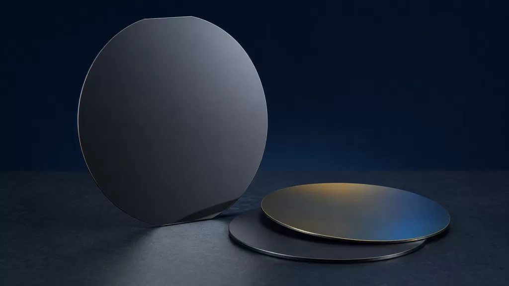
For research laboratories, epitaxy developers and established 100 mm production lines, 4-inch semi-insulating 4H-SiC wafers remain an important substrate format. Buyers should evaluate much more than wafer diameter and nominal resistivity before placing an order.
Why GaN RF Devices Use Semi-Insulating SiC
A typical GaN-on-SiC RF structure may contain:
- Semi-insulating 4H-SiC substrate
- AlN nucleation or transition layer
- GaN buffer layer
- GaN channel
- AlGaN or AlInN barrier
- Optional GaN or SiN cap layer
- Source, gate and drain structures
The semi-insulating substrate helps suppress parasitic electrical conduction below the active device layers. This is particularly important in coplanar waveguides, microstrip transmission lines, MMICs and high-frequency GaN HEMTs.
A suitable semi-insulating SiC substrate can provide:
- High electrical isolation
- Low substrate-related RF loss
- Высокая теплопроводность
- Good compatibility with GaN epitaxy
- High mechanical strength
- Stable performance at elevated temperatures
- Reduced crosstalk between adjacent RF devices
- Support for high-power-density operation
SiC also offers better heat spreading than many alternative substrate materials. However, the overall device temperature depends on both substrate thermal conductivity and thermal boundary resistance at the GaN/SiC interface. A poor nucleation layer or defective interface can partially offset the thermal benefits of SiC. Research on thermal boundary resistance in GaN-on-SiC devices
Typical 4-Inch Semi-Insulating SiC Wafer Configuration
The following table shows a commonly encountered configuration rather than a universal purchasing standard.
| Параметр | Typical selection for GaN-on-SiC RF |
|---|---|
| Диаметр | 100 mm, commonly called 4 inch |
| Polytype | Single-crystal 4H-SiC |
| Electrical type | High-purity semi-insulating or compensated semi-insulating |
| Сопротивление | Commonly specified at ≥1 × 10⁶ Ω·cm; higher values may be required |
| Surface orientation | (0001), often nominally on-axis |
| Front surface | Si-face |
| Полировка | Double-side polished or application-specific |
| Front surface finish | CMP polished, epi-ready |
| Толщина | Approximately 500 µm is common |
| Orientation feature | Primary and secondary flats |
| Класс | Research, production or customer-defined |
| Packaging | Semiconductor-compatible clean wafer cassette |
As one commercial reference, current 100 mm HPSI 4H-SiC products may be supplied on-axis, with resistivity of at least 1×1061 \times 10^61×106 Ω·cm, approximately 500 µm thickness and a CMP-finished Si-face. Exact tolerances vary by supplier and grade. Wolfspeed SiC materials catalog
1. Confirm 4H-SiC Polytype
Silicon carbide exists in many crystal structures, known as polytypes. For modern GaN-on-SiC RF applications, single-crystal 4H-SiC is generally the preferred substrate material.
The selected polytype affects:
- Crystal structure
- Полоса пропускания
- Thermal behavior
- Dielectric properties
- Surface preparation
- Epitaxial growth compatibility
The specification should explicitly state 4H-SiC rather than using the general term “SiC wafer.” Buyers should also request confirmation that the wafer is single-crystal material and that unwanted polytype inclusions are controlled.
Although 6H-SiC has historically been used in some high-frequency applications, it should not be substituted for 4H-SiC without confirming compatibility with the intended epitaxial process.
2. Evaluate Semi-Insulating Technology
The two major approaches to producing semi-insulating SiC are high-purity defect compensation and intentional deep-level compensation.
High-purity semi-insulating SiC
High-purity semi-insulating material is produced by reducing shallow electrically active impurities and controlling intrinsic defects that compensate residual carriers.
HPSI material is frequently requested for GaN RF substrates because it can combine high resistivity with low intentional dopant contamination. Some commercial HPSI products are specifically identified as vanadium-free.
Vanadium-doped semi-insulating SiC
Vanadium can introduce deep energy levels that compensate shallow donors or acceptors. Properly controlled vanadium doping can produce very high resistivity; experimental work has demonstrated vanadium-doped 4H-SiC material with resistivity above 101010^{10}1010 Ω·cm. Research on vanadium-doped semi-insulating 4H-SiC
However, buyers should evaluate:
- Vanadium concentration
- Resistivity uniformity
- Deep-level trap behavior
- Термическая стабильность
- Optical absorption
- Lot-to-lot consistency
- Compatibility with the GaN epitaxy process
Neither approach should be selected based only on the material name. The substrate must be evaluated against the electrical, thermal and RF requirements of the intended device.
3. Do Not Check Resistivity at Only One Point
Bulk resistivity is one of the most important parameters for a semi-insulating SiC wafer.
A common commercial threshold is: ρ≥1×10⁶ Ω⋅cm\rho \geq 1 \times 10^6\ \Omega\cdot\text{cm}ρ≥1×10⁶ Ω⋅cm
However, a single resistivity value does not fully describe RF substrate performance.
Buyers should confirm:
- Minimum resistivity
- Measurement method
- Measurement temperature
- Number of measurement points
- Radial resistivity distribution
- Center-to-edge uniformity
- Lot-to-lot consistency
- Stability after high-temperature processing
Local conductive regions can create microwave loss or device-to-device variation even when the average resistivity meets the specification.
If the substrate will be used for demanding microwave or millimeter-wave circuits, the buyer should also discuss RF dielectric loss rather than relying exclusively on DC resistivity.
4. Check Dielectric Constant and RF Loss
At high frequencies, the SiC substrate forms part of the RF electromagnetic environment. Its dielectric properties influence impedance, transmission-line design, signal propagation and substrate losses.
Important parameters include:
- Relative permittivity
- Dielectric loss tangent
- Permittivity anisotropy
- Frequency dependence
- Temperature dependence
- Wafer-to-wafer uniformity
4H-SiC has a hexagonal crystal structure, so its dielectric response can differ parallel and perpendicular to the c-axis. This anisotropy becomes increasingly important when designing microwave and millimeter-wave transmission structures.
Measurements of high-purity semi-insulating 4H-SiC have reported an extraordinary permittivity near 10.2 in the 110–170 GHz range, but buyers should use material data measured under conditions relevant to their own device design. Research on millimeter-wave permittivity of 4H-SiC
For RF substrate evaluation, ask the supplier whether dielectric data are available for:
- The intended frequency range
- Room and elevated temperatures
- The specific crystal orientation
- The required wafer grade
- Representative production lots
5. Select the Correct Surface Orientation
One common purchasing mistake is copying the orientation specification from a conductive SiC power-device wafer.
Conductive 4H-SiC substrates for homoepitaxial power devices are frequently supplied with a controlled off-axis angle, such as 4°. GaN heteroepitaxy on semi-insulating SiC, however, often uses nominally on-axis (0001) substrates.
The purchase specification should clearly define:
- Surface orientation
- On-axis or off-axis requirement
- Maximum orientation deviation
- Off-cut direction, if applicable
- Primary-flat orientation
- Front-surface polarity
A commercial 100 mm GaN-on-SiC substrate may, for example, specify a (0001) orientation with a limited angular tolerance. This value should not be assumed to apply to every supplier or epitaxial process.
Buyers should obtain the required orientation directly from the GaN epitaxy team before ordering.
6. Confirm Si-Face or C-Face
The basal surfaces of a 4H-SiC wafer are not chemically identical.
- Сайт Si-face is silicon-terminated.
- Сайт С-образная поверхность is carbon-terminated.
Most conventional Ga-polar GaN-on-SiC processes use a CMP-polished Si-face as the epitaxial growth surface. Specialized structures, including some N-polar GaN processes, may use different orientations or surface polarities.
The wafer documentation should identify:
- Front surface
- Back surface
- Polished face
- Laser-marking face
- Epitaxy-ready face
A request stating only “double-side polished SiC wafer” is incomplete if the front-surface polarity is not clearly identified.
7. Specify the Required Surface Finish
GaN epitaxy requires more than a visually shiny wafer. The front surface must be sufficiently smooth, clean and free from processing damage.
A suitable epi-ready surface should control:
- Шероховатость поверхности
- Царапины
- Pits
- Haze
- Stains
- Residual polishing marks
- Particles
- Metallic contamination
- Повреждения под поверхностью
Chemical mechanical polishing is commonly used to prepare the Si-face. CMP chemically modifies the hard SiC surface and gently removes the modified layer, reducing the damage left by slicing, grinding and mechanical polishing.
When reviewing a roughness value, buyers should also confirm:
- Ra or RMS measurement
- AFM scan area
- Number of test locations
- Center and edge results
- Maximum permitted local roughness
- Whether edge exclusion is applied
A roughness value without its measurement area and test method is difficult to compare between suppliers.
8. Check Thickness, TTV, Bow and Warp
Wafer geometry influences epitaxial growth, handling, lithography and RF fabrication.
Толщина
A thickness of approximately 500 µm is common for 100 mm semi-insulating SiC substrates, but the final requirement depends on the epitaxy reactor, handling system and device process.
Thicker wafers offer greater mechanical strength but may increase thermal path length. Thinner wafers may improve later-stage thermal resistance but can be more difficult to handle.
Total thickness variation
TTV represents the difference between the maximum and minimum wafer thickness. Excessive TTV can affect:
- Wafer chucking
- Epitaxial temperature uniformity
- Lithography focus
- Backside processing
- Device thickness control
Bow and warp
Bow describes overall central curvature, while warp evaluates the broader peak-to-valley deformation of the wafer.
Excessive bow or warp can result in:
- Unstable wafer handling
- Nonuniform thermal contact
- Epitaxial thickness variation
- Lithography focus errors
- Wafer breakage
- Difficulty during bonding or thinning
Buyers should specify numerical limits and measurement conditions instead of requesting only “good flatness.”
9. Review Crystal-Defect Specifications
Crystal defects in the SiC substrate can propagate into or influence the GaN epitaxial layer. They may also create local stress, leakage paths or unusable device areas.
Defects that may require evaluation include:
- Микротрубки
- Вывихи резьбовых винтов
- Threading edge dislocations
- Дислокации в базальной плоскости
- Low-angle grain boundaries
- Polytype inclusions
- Inclusions and precipitates
- Неисправности штабелирования
- Surface pits related to subsurface defects
Micropipe density is often used as a grade-related parameter, but it should not be the only defect specification.
Research and production grades may differ in:
- Permitted defect density
- Number of excluded regions
- Surface-defect limits
- Inspection coverage
- Mapping information
- Исключение краев
- Guaranteed usable area
For expensive epitaxial growth, requesting a wafer defect map can be more useful than receiving only a single average value.
10. Evaluate Thermal Conductivity
RF GaN HEMTs can generate high heat flux near the gate region. The substrate must spread this heat toward the package and cooling system.
High-purity semi-insulating 4H-SiC offers strong thermal conductivity compared with sapphire and many insulating substrate alternatives. One current commercial material reference reports room-temperature HPSI thermal conductivity of approximately:
- 4.9 W/cm·K along the a-axis
- 3.9 W/cm·K along the c-axis
These values correspond to approximately 490 and 390 W/m·K, respectively, but they should not be treated as universal guarantees for every wafer or supplier. SiC physical properties reference
The buyer should check:
- Thermal conductivity test method
- Crystal direction
- Test temperature
- Material grade
- Radial uniformity
- Impurity and defect effects
- Lot-specific data availability
The thermal performance of the completed device will also depend on nucleation layers, GaN buffer design, wafer thickness, backside processing, die attach and package design.
11. Check Frontside and Backside Requirements
For a double-side polished wafer, the buyer should specify whether both surfaces require the same finish.
Common configurations include:
- Si-face CMP polished and epi-ready
- C-face mechanically polished
- Double-side polished
- Frontside protected during backside processing
- Backside laser marked
- Unmarked wafer for specialized processing
Laser marking should normally be placed on the defined backside and outside the critical device area. Buyers should confirm marking content, character format, position and orientation.
If the wafer will later undergo thinning, backside metallization or temporary bonding, the backside roughness and contamination requirements may also be important.
12. Define Research and Production Grade
“Research grade” and “production grade” are not universal technical standards. Different suppliers may use the same grade names while applying different acceptance limits.
Buyers should compare the actual specifications for:
- Плотность микротрубок
- Плотность дислокаций
- Дефекты поверхности
- Resistivity uniformity
- TTV
- Bow and warp
- Краевые сколы
- Usable area
- Inspection coverage
- Traceability
- Lot consistency
Research-grade wafers may be suitable for epitaxy development, process trials, university research and equipment qualification. Production-grade wafers generally require tighter defect control, consistency and documentation.
The correct selection depends on whether the objective is material research, epitaxy optimization, device demonstration or volume RF manufacturing.
Recommended Purchasing Checklist
Before requesting a quotation, provide the following information:
| Артикул | Information to confirm |
|---|---|
| Диаметр | 100 mm or nominal 4 inch |
| Polytype | 4H-SiC |
| Electrical type | HPSI or vanadium-compensated semi-insulating |
| Сопротивление | Minimum value and uniformity requirement |
| Ориентация | On-axis or specified off-axis |
| Surface polarity | Si-face or C-face |
| Толщина | Nominal thickness and tolerance |
| TTV | Maximum acceptable value |
| Bow and warp | Maximum acceptable values |
| Полировка | SSP or DSP |
| Front surface | CMP polished and epi-ready |
| Шероховатость поверхности | Value, test method and AFM scan area |
| Defects | MPD and other dislocation limits |
| Thermal properties | Required test data, if applicable |
| RF properties | Permittivity or loss data, if required |
| Класс | Research, production or custom |
| Marking | Backside marking requirements |
| Quantity | Sample, pilot or production quantity |
| Documentation | Certificate of analysis and defect mapping |
Common Purchasing Mistakes
Selecting conductive N-type SiC
N-type SiC may be suitable for power devices but is generally inappropriate where the RF circuit requires an electrically isolating substrate.
Requesting only “high resistivity”
A minimum value does not describe radial uniformity, RF loss, temperature stability or deep-level behavior.
Using a 4° off-axis specification automatically
A 4° off-axis substrate is common in SiC homoepitaxy, but many GaN-on-SiC RF processes use nominally on-axis material.
Ignoring surface polarity
The supplier must know whether the Si-face or C-face is the required epitaxial surface.
Comparing roughness values without test conditions
AFM roughness values measured over different scan areas are not directly comparable.
Accepting a grade name without numerical limits
Always compare defect, geometry and surface specifications instead of relying only on “research” or “production” labels.
Заключение
The performance of a GaN-on-SiC RF device depends not only on the GaN epitaxial structure but also on the quality of the semi-insulating SiC substrate beneath it.
For 4-inch wafers, buyers should pay particular attention to resistivity uniformity, semi-insulating technology, surface orientation, polarity, CMP quality, TTV, bow, warp, crystal defects and thermal properties.
A complete purchasing specification helps prevent problems during GaN epitaxy, wafer handling and RF device fabrication. It also makes quotations from different SiC wafer suppliers easier to compare.
Frequently Asked Questions
Why not use conductive SiC for GaN RF devices?
Conductive SiC can allow parasitic substrate currents and increase RF losses. Semi-insulating SiC provides electrical isolation while maintaining high thermal conductivity.
What resistivity is required?
A common commercial specification is at least 1×1061 \times 10^61×106 Ω·cm. More demanding RF applications may require higher resistivity, tighter uniformity or additional dielectric-loss data.
Should a GaN-on-SiC wafer be on-axis or off-axis?
Many GaN RF epitaxy processes use nominally on-axis (0001) 4H-SiC. The correct orientation must be confirmed with the epitaxy provider.
Is HPSI always better than vanadium-doped SiC?
Not automatically. HPSI avoids intentional vanadium in some commercial products, while controlled vanadium compensation can achieve very high resistivity. The best choice depends on resistivity uniformity, RF loss, thermal stability and epitaxial compatibility.
Is double-side polishing necessary?
It depends on the process. Double-side polishing can improve handling, backside inspection and geometric control, while some applications only require an epi-ready CMP front surface.
What information is needed for a quotation?
At minimum, provide diameter, polytype, semi-insulating method, resistivity, orientation, thickness, polishing, surface roughness, TTV, bow, warp, grade, quantity and packaging requirements.