
Описание
1. Product Overview
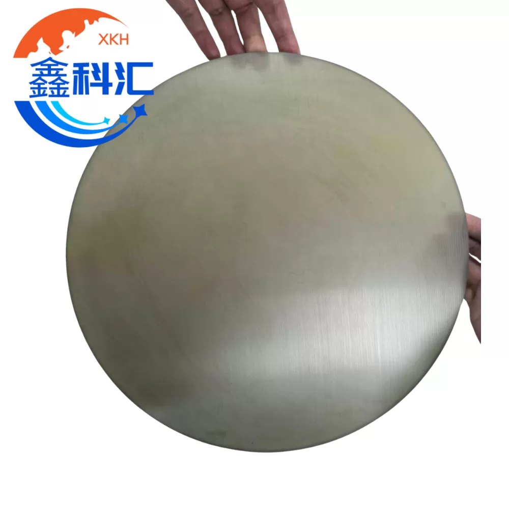
The 12-inch 4H-N silicon carbide (SiC) substrate is a premium material platform engineered for the most demanding applications in power electronics, high-voltage devices, and RF/microwave components. Leveraging the superior thermal conductivity, wide bandgap, and high breakdown voltage of SiC, these substrates enable next-generation semiconductor devices to achieve higher efficiency, reduced energy loss, and enhanced reliability under extreme operating conditions.
We provide both production-grade и dummy-grade wafers to support a wide range of applications:
Production-grade wafers: Optimized for device fabrication, epitaxial growth, and mass production processes.
Dummy-grade wafers: Designed for equipment calibration, process tuning, and non-device runs, where surface perfection and defect control are less critical.
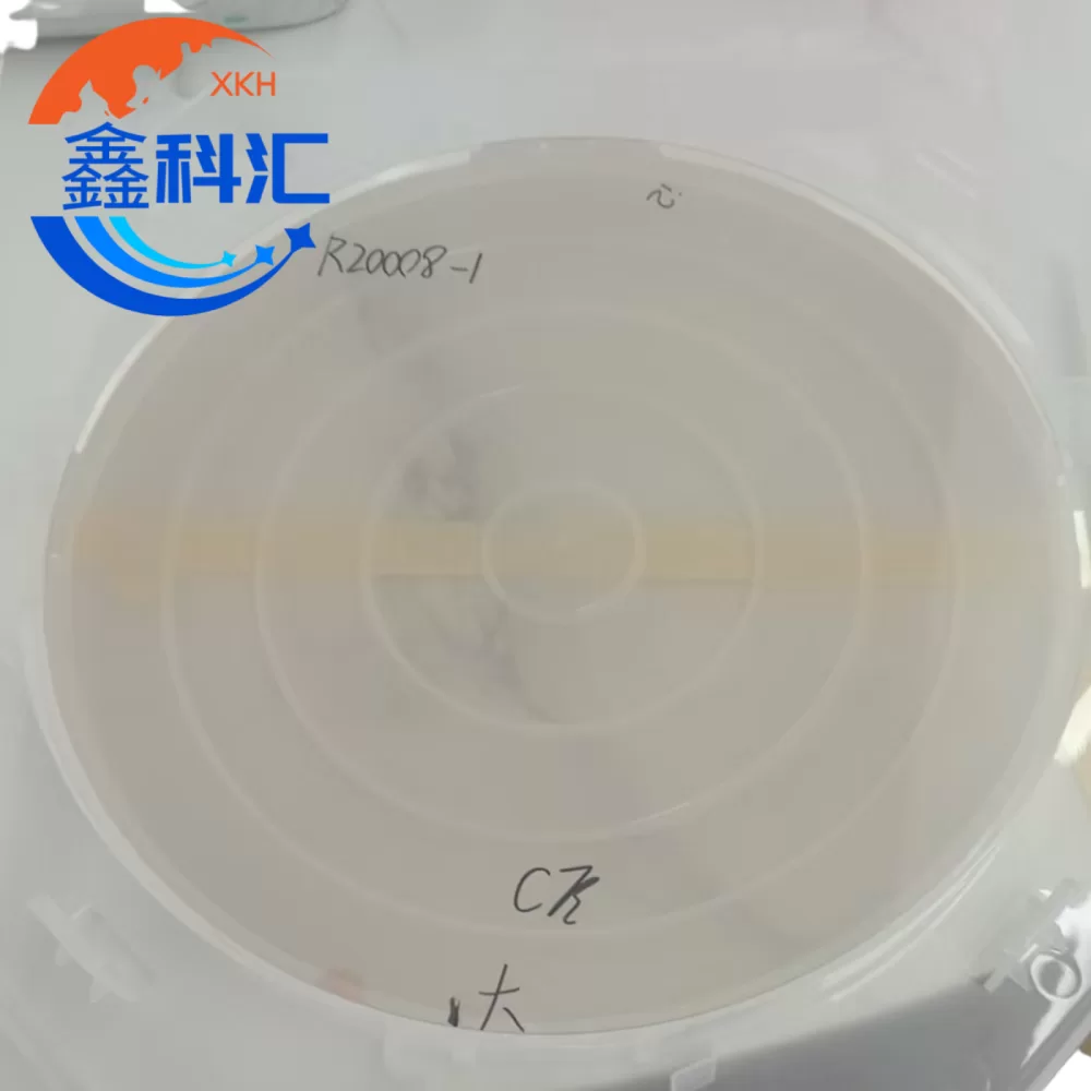
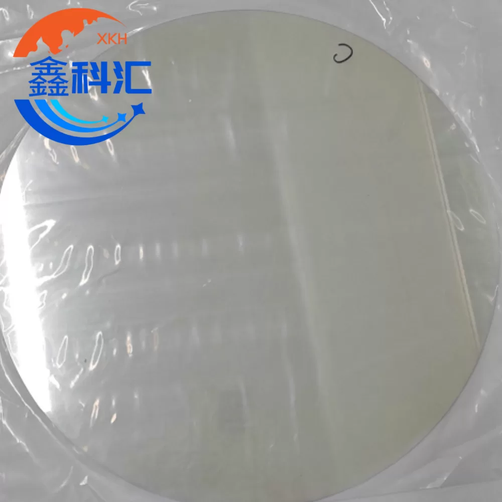
Available in both green (600 μm) и transparent (700 μm) thicknesses, these wafers can meet diverse process requirements and are compatible with standard 12-inch semiconductor processing equipment.

2. 12-Inch Silicon Carbide Substrate Specification
| Артикул | N-type Production Grade | N-type Dummy Grade | SI-type Production Grade |
|---|---|---|---|
| Crystal Structure (Polytype) | 4H-N SiC | 4H-N SiC | 4H SiC |
| Doping Type | N-тип | N-тип | / |
| Диаметр | 300 ± 0.5 mm | 300 ± 0.5 mm | 300 ± 0.5 mm |
| Толщина | Green: 600 ± 100 μm / Transparent: 700 ± 100 μm | Same as Production | Same as Production |
| Surface Orientation | 4° toward <11-20> ± 0.5° | Same | Same |
| Primary Flat / Notch | Notch / Full Round | Notch / Full Round | Notch / Full Round |
| Notch Depth | 1.0 – 1.5 mm | 1.0 – 1.5 mm | 1.0 – 1.5 mm |
| TTV (Total Thickness Variation) | ≤ 10 μm | NA | ≤ 10 μm |
| Micropipe Density (MPD) | ≤ 5 ea/cm² | NA | ≤ 5 ea/cm² |
| Resistivity Measurement | Measured at central 8-inch equivalent zone | NA | Measured at central 8-inch equivalent zone |
| Si-Surface Treatment | CMP Polished | Grinding | CMP Polished |
| Edge Processing | Chamfer | No Chamfer | Chamfer |
| Edge Chips | Allowed depth < 0.5 mm | Allowed depth < 1.0 mm | Allowed depth < 0.5 mm |
| Laser Marking | C-side marking / Customer specified | C-side marking | C-side marking / Customer specified |
| Polytype Inspection (Polarized Light) | No polytype (3 mm edge exclusion) | Polytype area < 5% (3 mm edge exclusion) | No polytype (3 mm edge exclusion) |
| Crack Inspection (High-Intensity Light) | No cracks (3 mm edge exclusion) | Not specified | No cracks (3 mm edge exclusion) |
3. Grade Definition
Производственный класс
Production-grade wafers meet the highest standards of dimensional uniformity, surface quality, and defect control. They are suitable for:
Epitaxial layer growth for SiC power devices
High-voltage and high-frequency device fabrication
Mass production lines requiring tight TTV, low micropipe density, and strict crack control
Фиктивная оценка
Dummy-grade wafers are intended for:
Equipment setup and calibration
Process development and optimization
Non-device runs where surface polishing, chamfering, and micropipe control are non-critical

4. Inspection & Quality Assurance
All production-grade wafers undergo rigorous inspection to ensure reliability and consistency:
Polytype verification using polarized light microscopy to ensure crystal uniformity
Crack detection with high-intensity light to identify micro-cracks
Dimensional verification: diameter, thickness, and total thickness variation (TTV)
Surface and edge assessment: evaluating edge chamfer, chipping, and surface polish quality
Inspection zones exclude a 3 mm edge margin, consistent with industry standards, ensuring that the wafer interior meets precise electrical and mechanical specifications.
5. Typical Applications
SiC Power Devices: MOSFETs, diodes, and IGBTs
High-Voltage Applications: Automotive, industrial, and renewable energy inverters
RF and Microwave Devices: Semi-insulating (SI) wafers for RF, microwave, and high-frequency applications
Process Development & Equipment Qualification: Using dummy wafers for calibration, laser tuning, and prototype runs
6. Frequently Asked Questions (FAQ)
Q1: What is the difference between 4H-N SiC and SI-type 4H SiC?
4H-N SiC is N-type conductive material ideal for power devices, while SI-type 4H SiC is semi-insulating, used mainly in RF and high-frequency applications.
Q2: Why measure resistivity in the central 8-inch equivalent zone?
The central region of a 12-inch wafer offers the most uniform electrical properties. Measuring this zone ensures stable and comparable resistivity across wafers.
Q3: Can the notch orientation or laser marking be customized?
Yes. Both notch configuration and laser marking content can be customized to meet specific customer requirements.
Q4: Are dummy wafers suitable for epitaxy or device fabrication?
No. Dummy wafers are designed solely for equipment setup and process testing, not for device production.
Q5: What edge quality is guaranteed for production wafers?
Production-grade wafers feature chamfered edges with edge chipping depth ≤ 0.5 mm for safe handling and process compatibility.
Q6: Are green and transparent wafers available?
Yes. Green wafers (600 μm) and transparent wafers (700 μm) are available depending on processing needs.
Q7: Can the wafers be used in extreme high-temperature or high-voltage processes?
Absolutely. 4H-N SiC substrates provide superior thermal conductivity and electrical stability, making them ideal for high-temperature, high-voltage, and high-frequency device manufacturing.


Отзывы
Отзывов пока нет.