
Описание
As advanced semiconductor packaging moves toward higher integration density, larger package sizes, and thinner wafer structures, maintaining dimensional stability throughout the manufacturing process has become increasingly challenging. Temporary wafer carriers play a critical role in supporting ultra-thin wafers during grinding, thinning, bonding, debonding, and backside processing operations.
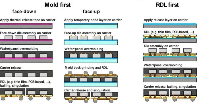
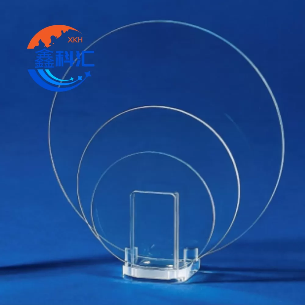
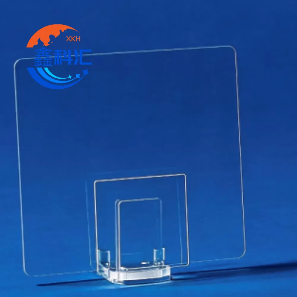
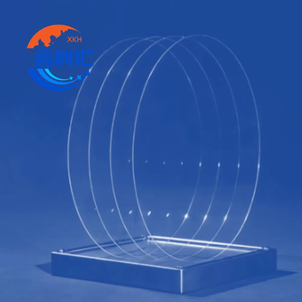
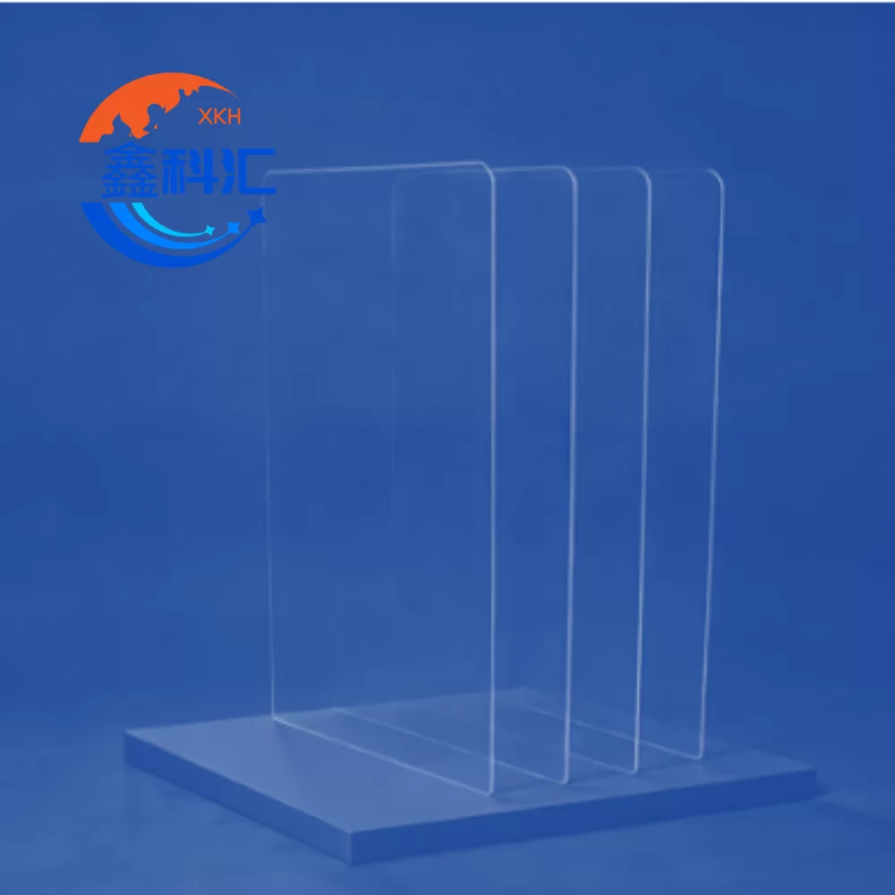
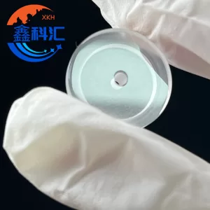
The Sapphire Temporary Wafer Carrier is specifically developed for advanced packaging applications requiring superior warpage control, mechanical rigidity, and process stability. Leveraging sapphire’s unique combination of high modulus, excellent optical transmission, and outstanding material uniformity, the carrier provides reliable support for next-generation packaging technologies, including 2.5D/3D IC, TSV, RDL, and Fan-Out Packaging.
 Why Sapphire for Temporary Carriers?
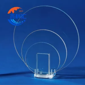 Why Sapphire for Temporary Carriers?
Traditional carrier materials such as glass and silicon often face limitations when processing increasingly thin wafers and complex package structures. Differences in thermal expansion coefficients between packaging materials can generate significant stress during thermal cycling, leading to deformation, warpage, and yield loss.
Sapphire offers a unique solution through its exceptional physical properties:
- High rigidity to minimize wafer deformation
- Excellent dimensional stability during thermal processing
- High optical transparency for laser debonding compatibility
- Superior surface durability for repeated use
- Uniform material characteristics for consistent process performance
These advantages make sapphire an attractive carrier material for advanced semiconductor manufacturing environments.
Key Features & Benefits
Excellent Warpage Control
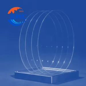 Excellent Warpage Control
With a Young’s Modulus ranging from 345 to 420 GPa, sapphire provides significantly higher stiffness than conventional glass carriers. This helps suppress package deformation and maintain wafer flatness throughout thermal and mechanical processing steps.
Laser Debonding Compatibility
Sapphire exhibits optical transmittance greater than 83% across the 300–1200 nm wavelength range, making it highly suitable for laser-assisted debonding processes commonly used in advanced packaging production.
Высокая механическая прочность
The combination of high hardness and strength allows sapphire carriers to provide stable support for fragile ultra-thin wafers, reducing breakage risks during handling and transportation.
Superior Surface Quality
Advanced polishing technologies enable ultra-low surface roughness and excellent thickness uniformity, supporting high-precision semiconductor manufacturing requirements.
Outstanding Reliability
Excellent thermal and chemical stability ensures consistent performance under demanding process environments, including high-temperature cycling and chemical cleaning operations.
Технические характеристики
Available Dimensions
| Артикул | Технические характеристики |
|---|---|
| Wafer Formats | 8″ / 12″ |
| Panel Formats | 100 × 100 mm to 510 × 515 mm |
| Thickness Range | 0.7 – 2.0 mm |
Precision Specifications
| Параметр | Standard Grade | Advanced Grade |
| Total Thickness Variation (TTV) | ≤ 3 μm | ≤ 2 μm |
| Warp | ≤ 100 μm | ≤ 50 μm |
| Допуск по толщине | ±0.010 mm | ±0.005 mm |
| Шероховатость поверхности (Ra) | < 1.0 nm | < 1.0 nm |
| Scratch/Dig | 60/40 | 40/20 |
Material Properties
| Недвижимость | Значение |
| Young’s Modulus | 345 – 420 GPa |
| Vickers Hardness | 1800 – 2200 HV |
| Optical Transmittance | >83% (300–1200 nm) |
| Теплопроводность | 30 – 40 W/m·K |
| Плотность | 3,98 г/см³ |
| Coefficient of Thermal Expansion (CTE) | 5.6 – 7.7 × 10⁻⁶/K |
Typical Applications
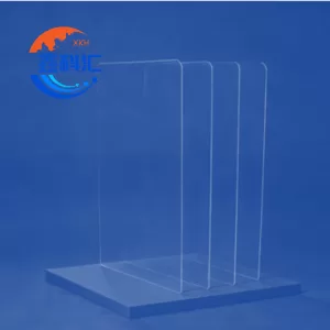 Typical Applications
- Temporary wafer bonding and debonding
- Wafer thinning processes
- Through-Silicon Via (TSV) fabrication
- Redistribution Layer (RDL) processing
- 2.5D and 3D IC packaging
- Fan-Out Wafer Level Packaging (FOWLP)
- Fan-Out Panel Level Packaging (FOPLP)
- Heterogeneous integration technologies
- High-performance computing (HPC) packaging
- AI accelerator and HBM packaging platforms
Параметры настройки
Customized sapphire carriers are available to meet specific process requirements.
Customization capabilities include:
- Custom wafer diameters and panel dimensions
- Оптимизация толщины
- Precision flatness specifications
- Surface finish requirements
- Edge profile design
- Advanced optical and surface quality standards
ЧАСТО ЗАДАВАЕМЫЕ ВОПРОСЫ
Q1: What are the main advantages of sapphire compared with glass carriers?
Sapphire offers significantly higher stiffness, hardness, and mechanical strength than glass, enabling better warpage suppression and improved stability during ultra-thin wafer processing.
Q2: Is sapphire suitable for laser debonding applications?
Yes. Sapphire provides excellent optical transmission across UV, visible, and infrared wavelengths, making it highly compatible with laser debonding technologies.
Q3: Can sapphire carriers be customized for panel-level packaging?
Yes. Sapphire carriers can be manufactured in both wafer and large-panel formats with customized dimensions, thicknesses, and precision specifications according to customer requirements.

Отзывы
Отзывов пока нет.