
AI data centers are rapidly moving toward higher rack power, higher power density and more efficient electrical distribution.
One of the most important changes is the emergence of 800 VDC power architectures.
NVIDIA is developing 800 VDC infrastructure for next-generation AI factories as traditional low-voltage rack distribution becomes increasingly difficult to scale to hundreds of kilowatts and eventually megawatt-class racks. NVIDIA states that 800 VDC reduces current, conductor requirements and conversion stages while supporting much higher compute density.
This transition also creates new opportunities for wide-bandgap power semiconductors.
In June 2026, Infineon introduced a 24 kW battery backup unit reference design connected directly to an 800 VDC bus using 650 V and 1200 V SiC devices, reporting efficiency above 99%. In September 2026, Infineon and SolarEdge also announced work on solid-state circuit breakers for high-voltage DC AI data centers using SiC JFET technology.
But the discussion should not stop at the MOSFET or JFET level.
The performance and reliability of these devices ultimately depend on the quality of the 4H-SiC substrate and epitaxial wafer underneath them.
For SiC wafer suppliers, the growth of 800 VDC AI infrastructure raises important questions:
- What substrate resistivity is required?
- How uniform must the epitaxial layer be?
- Which crystal and epi defects matter most?
- How do BPD, TSD, TED and surface defects influence device reliability?
- Which wafer parameters should buyers specify for 650 V, 1200 V and higher-voltage power devices?
- How should SiC wafers be qualified for continuous high-power data-center operation?
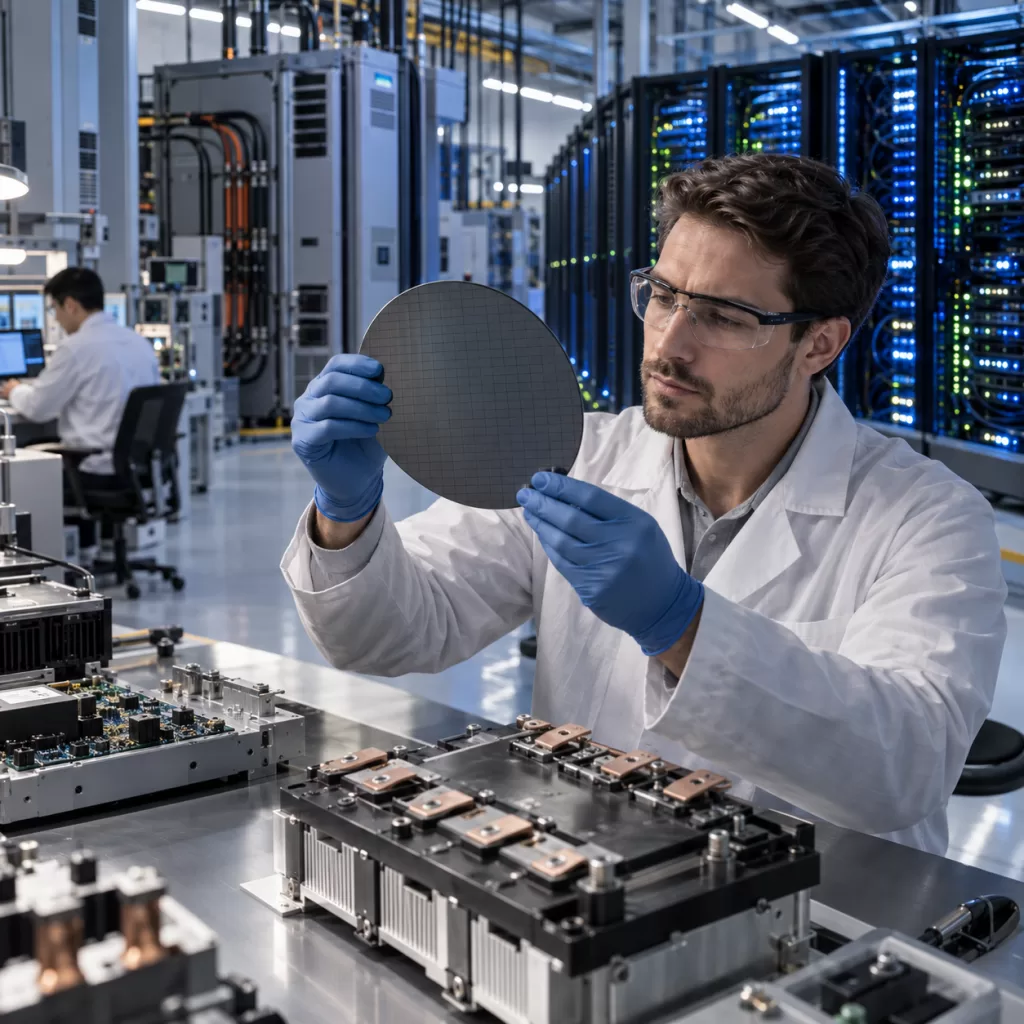
Why AI Data Centers Are Moving Toward 800 VDC
Traditional server racks distribute relatively low DC voltages close to the computing hardware.
That architecture becomes increasingly difficult as rack power rises.
For a simplified power relationship:
Power = Voltage × Current
Delivering the same amount of power at a higher voltage reduces current.
Lower current can reduce:
- conductor cross-section,
- copper consumption,
- resistive losses,
- cable volume,
- busbar size,
- thermal load.
This becomes particularly important as AI infrastructure moves toward several hundred kilowatts per rack.
NVIDIA’s roadmap describes future architectures supporting 1 MW-class racks and beyond, with 800 VDC distributed much closer to the compute equipment instead of repeatedly converting power through multiple AC and low-voltage DC stages.
Infineon similarly describes next-generation racks above approximately 500 kW moving toward high-voltage DC sidecar architectures, with larger systems eventually using facility-level 800 VDC distribution.
Where SiC Devices Fit Into an 800 VDC Data Center
It is important not to assume that every semiconductor switch inside an 800 VDC data center will be SiC.
Different semiconductor materials may be optimized for different parts of the power chain.
A simplified architecture may include:
Grid → AC/DC Conversion → 800 VDC Distribution → Protection → Battery Backup → Intermediate Conversion → GPU Power
Depending on voltage, frequency and power density, this system may combine:
- silicon,
- silicon carbide,
- gallium nitride.
SiC becomes particularly attractive where designers require a combination of:
- high blocking voltage,
- high efficiency,
- high power density,
- fast switching,
- lower switching losses,
- high-temperature capability.
Infineon describes SiC as particularly suitable for high-efficiency, high-voltage portions of the grid-to-rack power chain, while GaN can serve high-frequency intermediate conversion stages.
Potential SiC applications include:
- front-end power conversion,
- high-voltage DC/DC conversion,
- battery backup units,
- solid-state circuit breakers,
- hot-swap protection,
- solid-state transformers,
- high-voltage auxiliary power systems.
Why an 800 VDC Bus Often Leads to 1200 V-Class SiC Devices
An 800 VDC bus does not mean that every switching device should have an 800 V blocking rating.
Power semiconductor designers require voltage margin for:
- switching overshoot,
- parasitic inductance,
- transient events,
- fault conditions,
- control tolerance,
- long-term reliability.
This is one reason why 1200 V SiC MOSFETs and related devices are important candidates for high-voltage data-center power conversion.
However, topology matters.
Some multilevel architectures can use lower-voltage devices such as 650 V switches, while other stages may use 1200 V or potentially higher-voltage SiC devices.
Infineon’s 800 VDC BBU reference design, for example, combines 650 V and 1200 V SiC technology rather than relying on one device voltage class throughout the system.
Therefore, wafer requirements should always be defined from the actual device architecture rather than simply stating:
SiC wafer for 800 VDC.
1. Why the SiC Substrate Still Matters
A vertical SiC power MOSFET generally consists of several functional layers.
A simplified structure includes:
Metal / Source Structure
↓
Channel and Body Region
↓
SiC Epitaxial Drift Layer
↓
4H-SiC Substrate
↓
Backside Drain Contact
The substrate provides:
- mechanical support,
- crystal template for epitaxy,
- electrical conduction toward the backside contact,
- thermal conduction.
For conductive vertical devices, the substrate is commonly N-type 4H-SiC.
Important substrate parameters include:
- polytype,
- orientation,
- off-cut,
- resistivity,
- resistivity uniformity,
- thickness,
- TTV,
- bow,
- warp,
- BPD density,
- TSD/TED density,
- micropipe density,
- surface quality.
2. Substrate Resistivity: Lower Is Not Always the Whole Story
For vertical SiC power devices, current passes through the substrate.
Substrate electrical resistance therefore contributes to the total conduction resistance of the device.
A lower-resistivity N-type substrate can help reduce substrate contribution to:
RDS(on)
which is important in high-current power conversion.
However, substrate specification should not be reduced to:
Lowest resistivity available.
The device manufacturer must also consider:
- resistivity uniformity,
- dopant concentration,
- wafer-to-wafer repeatability,
- crystal quality,
- compensation,
- defect interactions,
- backside contact processing.
A supplier may specify a resistivity range, but production buyers should also ask:
- How many points are measured?
- Is a resistivity map available?
- What is the center-to-edge variation?
- What is the lot-to-lot distribution?
For large-area 150 mm and 200 mm wafers, uniformity can become just as important as the nominal resistivity value.
3. Why Resistivity Uniformity Matters for AI Power Devices
AI data centers operate large numbers of power devices in parallel.
If device electrical characteristics vary significantly, this can complicate:
- current sharing,
- thermal management,
- module matching,
- system efficiency.
Not all device variation originates from the substrate, but substrate resistivity consistency is one component of the overall process-control chain.
For production-grade SiC wafers, buyers should therefore evaluate:
Nominal Resistivity + Within-Wafer Uniformity + Wafer-to-Wafer Uniformity + Lot-to-Lot Stability
rather than one resistivity number.
4. The Epitaxial Layer Determines the High-Voltage Drift Region
For many vertical SiC power devices, the most important voltage-blocking region is not the substrate itself.
It is the epitaxial drift layer grown on top of the substrate.
The required epi design depends strongly on device voltage.
Important parameters include:
- epitaxial thickness,
- doping concentration,
- doping uniformity,
- thickness uniformity,
- crystal defects,
- surface morphology.
In general, higher blocking voltage requires changes in drift-layer thickness and doping.
The exact values depend on:
- MOSFET architecture,
- cell design,
- termination design,
- target breakdown voltage,
- desired RDS(on),
- reliability margin.
Therefore, an RFQ for a SiC epitaxial wafer should not merely request:
1200 V epi wafer.
Instead it should specify measurable material parameters.
5. Typical Information Needed for a 1200V-Class SiC Epi RFQ
A practical RFQ may include:
Substrate
- 4H-SiC
- N-type
- wafer diameter
- off-axis orientation
- substrate resistivity
- thickness
- TTV
- bow
- warp
- surface condition
Epitaxy
- epi thickness
- thickness tolerance
- thickness uniformity
- net carrier concentration
- doping tolerance
- doping uniformity
- surface roughness
- BPD requirement
- surface defect specification
- edge exclusion
- usable area
The actual numbers should be determined by the device manufacturer.
6. Epi Thickness Uniformity Becomes Critical on 200mm Wafers
The SiC industry is transitioning from 150 mm toward 200 mm wafers.
This increases the importance of across-wafer epitaxial uniformity.
Suppose the drift layer thickness varies significantly from:
center → middle → edge.
The electrical characteristics of dies from different locations may then vary.
Possible consequences include changes in:
- breakdown voltage,
- conduction resistance,
- device matching,
- production yield.
For AI data-center power systems involving very large numbers of devices, tighter electrical distributions can become increasingly valuable.
Therefore, an epi-wafer CoA should ideally contain actual mapping or uniformity information rather than simply:
Thickness: PASS.
7. Epitaxial Doping Uniformity Is Equally Important
Drift-layer doping influences the balance between:
- blocking capability,
- electric-field distribution,
- specific on-resistance.
Poor doping uniformity can lead to wafer-level variation in device characteristics.
Production qualification should therefore evaluate:
Within-wafer doping uniformity
as well as:
wafer-to-wafer repeatability.
For 200 mm SiC, reactor uniformity becomes an increasingly important issue because the growth process must control gas distribution and temperature across a much larger surface.
8. Defect Density Is Not Just a Yield Number
One of SiC’s biggest manufacturing challenges is crystalline defects.
Relevant defects include:
- micropipes,
- basal plane dislocations,
- threading screw dislocations,
- threading edge dislocations,
- stacking faults,
- triangular defects,
- carrot defects,
- downfall defects,
- surface pits.
These defects do not all have the same impact.
Some may have limited influence on a particular device design.
Others can become killer defects that reduce yield or long-term reliability.
Recent SiC research continues to identify defects in both substrates and epitaxial layers as critical constraints on power-device performance and reliability.
9. Why BPD Control Matters
Basal Plane Dislocations — BPDs are particularly important in SiC power devices.
BPD-related stacking-fault expansion has historically been associated with bipolar degradation.
Research has shown that BPDs and related stacking faults can influence forward conduction and long-term electrical behavior.
Modern epitaxial processes attempt to control BPD propagation and promote conversion into less harmful defect configurations.
For wafer qualification, buyers may therefore ask:
- substrate BPD density,
- epi BPD density,
- BPD conversion performance,
- photoluminescence maps,
- defect classification method.
For applications where body-diode operation is important, these parameters deserve particular attention.
10. TSD and TED Should Not Be Ignored
Threading defects include:
TSD — Threading Screw Dislocation
and
TED — Threading Edge Dislocation
Their densities can be considerably higher than micropipe density.
Research indicates that threading dislocations and associated surface features may affect leakage, oxide reliability and device performance under high-voltage stress.
This means that a modern SiC specification cannot rely on the historical metric:
MPD — Micropipe Density
alone.
A more meaningful defect evaluation should consider multiple defect families.
11. Surface Defects Can Become Device-Killing Defects
Epitaxial growth can generate surface defects including:
- triangular defects,
- carrots,
- pits,
- downfall defects.
These defects are particularly important because they may intersect active device regions.
Recent studies have linked triangular and related epi defects with abnormal leakage or degraded electrical behavior in SiC power devices.
Therefore, buyers should ask not only:
What is the total defect density?
but:
What types of defects are included in that number?
12. Ask for a Defect Map
An average defect-density specification can hide spatial information.
For example:
Wafer A: defects evenly distributed.
Wafer B: same average density but concentrated in one quadrant.
From a device-layout and die-yield perspective, these wafers may behave very differently.
A defect map can show:
- center-to-edge patterns,
- clusters,
- crystal growth sectors,
- local epi abnormalities,
- repeatable reactor signatures.
For qualification of high-value 200 mm epi wafers, defect mapping is increasingly valuable.
13. Why Wafer Flatness Matters
AI data-center applications do not create a special TTV specification by themselves.
However, production of high-performance SiC devices requires stable wafer geometry.
Important parameters include:
- TTV,
- bow,
- warp,
- local shape,
- edge roll-off.
Poor wafer geometry can influence:
- epitaxial growth,
- wafer handling,
- lithography,
- implantation,
- metallization,
- wafer thinning,
- backside processing.
This becomes particularly important when moving from 150 mm to 200 mm SiC wafers.
SEMI’s work on 200 mm SiC wafer specifications has specifically addressed physical characteristics including thickness, flatness, orientation and defects.
14. Why AI Data Centers Raise the Reliability Bar
A power device inside an AI data center may operate for very long periods under:
- high voltage,
- high current,
- elevated junction temperature,
- frequent load changes,
- switching transients.
AI workloads can also change power demand rapidly.
NVIDIA has highlighted large and fast power variations as an infrastructure challenge for AI factories.
This means data-center power electronics must combine:
Efficiency + Power Density + Reliability
rather than optimize only one.
15. Important SiC Device Reliability Tests
Relevant qualification may include:
HTRB
High Temperature Reverse Bias
Evaluates blocking reliability under elevated temperature and high drain voltage.
HTGB
High Temperature Gate Bias
Evaluates gate-oxide stability.
TDDB
Time-Dependent Dielectric Breakdown
Evaluates long-term gate dielectric reliability.
UIS
Unclamped Inductive Switching
Evaluates avalanche robustness.
Short-Circuit Testing
Evaluates device survival during abnormal high-current events.
Power Cycling
Evaluates repeated thermo-mechanical stress.
Body-Diode Reliability
Important where reverse conduction occurs through the MOSFET body diode.
Modern studies of SiC MOSFET reliability continue to focus on gate-oxide degradation, threshold-voltage drift, avalanche behavior, body-diode degradation and other high-field stress mechanisms.
16. Reliability Starts Before Device Fabrication
Device reliability is often discussed as if it begins at the MOSFET fabrication stage.
In reality, the chain begins earlier:
Crystal Growth
↓
Substrate Processing
↓
CMP
↓
Epitaxy
↓
Device Fabrication
↓
Packaging
↓
Power Module
↓
800 VDC System
A material defect introduced near the beginning of this chain can influence downstream yield or reliability.
This is why substrate and epi suppliers increasingly need to provide:
- defect maps,
- wafer-level data,
- CoA,
- lot IDs,
- boule traceability,
- process-change control.
17. Recommended CoA Data for AI Power SiC Wafers
A substrate CoA may include:
Substrate
- wafer ID,
- lot number,
- boule number,
- diameter,
- thickness,
- TTV,
- bow,
- warp,
- resistivity,
- orientation,
- off-cut,
- surface roughness.
Crystal Defects
- micropipes,
- BPD,
- TSD,
- TED,
- other agreed defects.
Epitaxy
- epi thickness,
- thickness uniformity,
- doping,
- doping uniformity,
- surface defect density,
- BPD-related data,
- particle data.
Actual measured values are generally more useful than simple PASS/FAIL statements.
18. 150mm vs 200mm SiC for AI Data-Center Power
Today, both wafer sizes may remain relevant depending on the device manufacturer and production line.
150mm
Advantages may include:
- mature manufacturing ecosystem,
- established device processes,
- extensive qualification history.
200mm
Potential advantages include:
- more dies per wafer,
- better long-term manufacturing economics,
- compatibility with larger-wafer fabs,
- potential for higher production capacity.
However, 200 mm does not automatically guarantee lower cost.
The economic advantage depends on:
- crystal yield,
- wafer yield,
- epi yield,
- defect density,
- device yield,
- equipment utilization.
For power-semiconductor manufacturers, qualified usable die per wafer ultimately matters more than wafer diameter alone.
19. What an AI Data-Center SiC Wafer Buyer Should Specify
A practical RFQ should define the intended device.
For example:
Application: 800 VDC AI Data Center Power Conversion
Device: 1200 V-Class SiC MOSFET
Polytype: 4H-SiC
Conductivity: N-Type
Diameter: 150 mm / 200 mm
Orientation: Customer-defined
Off-Cut: Customer-defined
Substrate Resistivity: Defined range
Thickness: Defined value
TTV: Maximum limit
Bow: Maximum limit
Warp: Maximum limit
Surface: Si-Face CMP
Epitaxy: Required / Not Required
Epi Thickness: Device-design dependent
Epi Doping: Device-design dependent
Thickness Uniformity: Defined maximum
Doping Uniformity: Defined maximum
Defects: BPD/TSD/TED and surface-defect requirements
Mapping: Requested
Documentation: CoA + wafer ID + lot traceability
This creates a much more meaningful inquiry than simply asking:
Please quote SiC wafers for AI servers.
20. Do Not Specify the Wafer From the “800V” Number Alone
One common misunderstanding should be avoided.
An 800 VDC data-center bus voltage does not directly determine the SiC wafer specification.
The correct chain is:
System Voltage
→ Converter Topology
→ Device Blocking Voltage
→ Device Architecture
→ Drift Layer Design
→ Epitaxy Specification
→ Substrate Specification
For example, two converters connected to the same 800 VDC bus could use different:
- voltage classes,
- device topologies,
- switching frequencies,
- series/parallel configurations,
- epi structures.
Their wafer requirements may therefore be different.
21. SiC Is Also Becoming Important for 800VDC Protection
Power conversion is not the only emerging SiC application.
In September 2026, Infineon and SolarEdge announced work on solid-state circuit breakers for high-voltage DC AI data centers, with Infineon’s SiC JFET technology used in the protection architecture.
This is significant because fault interruption in DC systems is more difficult than in conventional AC distribution.
There is no natural zero-current crossing every half-cycle.
High-voltage DC infrastructure therefore needs extremely fast and reliable fault isolation.
For SiC, this expands the potential market from:
energy conversion
into:
power distribution and protection.
22. Material Consistency May Become More Important Than Peak Specifications
As AI data centers move toward extremely high power levels, power-semiconductor manufacturers may consume very large quantities of devices.
This shifts the focus from demonstrating the best individual wafer to achieving:
- wafer-to-wafer consistency,
- lot-to-lot consistency,
- stable defect distribution,
- predictable epi performance,
- reliable traceability.
For production applications, a wafer with slightly better headline parameters but poor lot stability may be less useful than a consistently controlled production process.
Therefore, SiC suppliers should increasingly focus on:
Process Capability rather than Sample Capability.
Conclusion
The move toward 800 VDC AI data-center power architectures is creating a new high-power application space for SiC semiconductors.
SiC devices can contribute to:
- high-voltage AC/DC conversion,
- DC/DC conversion,
- battery backup,
- solid-state circuit protection,
- high-efficiency power distribution.
But device-level performance begins with material quality.
For SiC substrates and epitaxial wafers, important parameters include:
substrate resistivity, resistivity uniformity, epi thickness, doping uniformity, BPD, TSD, TED, surface-defect density, TTV, bow, warp and lot traceability.
The central requirement is not simply to provide a wafer capable of producing a high-voltage device.
It is to provide wafers that repeatedly support:
low conduction loss + high breakdown capability + high manufacturing yield + long-term reliability.
As 800 VDC architectures move from reference designs toward wider deployment, the connection between AI infrastructure and SiC material quality will become increasingly important.
For wafer suppliers, this creates an opportunity to move beyond selling generic 4H-SiC substrates and toward providing application-qualified SiC material for next-generation high-voltage power systems.
FAQ
Why is SiC suitable for 800 VDC AI data centers?
SiC power devices combine high blocking voltage, low switching losses, high-temperature capability and high power density. These characteristics make SiC attractive for high-voltage conversion, battery backup and protection stages in emerging 800 VDC architectures.
Does an 800 VDC data center require 1200 V SiC MOSFETs?
Not necessarily in every conversion stage. The required device voltage depends on topology, transient margin and system design. Current 800 VDC reference designs can combine different device voltage classes; Infineon’s 24 kW BBU, for example, uses both 650 V and 1200 V SiC technology.
What SiC wafer defects are most important for power devices?
Important defects include micropipes, BPDs, TSDs, TEDs, stacking faults and epitaxial surface defects such as triangular and carrot-type defects. Their impact varies according to device architecture, so defect type and distribution should be evaluated rather than relying only on a single total defect-density value.
Why does SiC epitaxy matter for a 1200 V power device?
The epitaxial drift layer is a major part of the voltage-blocking structure. Epi thickness, doping concentration, uniformity and defect density therefore directly influence the manufacturability and electrical characteristics of high-voltage SiC devices.
Should buyers choose 150mm or 200mm SiC wafers for AI power devices?
The correct choice depends on the manufacturer’s qualified production line. 200 mm offers potential manufacturing-scale advantages, while 150 mm currently benefits from a more mature production history. The relevant comparison is qualified device yield and total manufacturing cost rather than diameter alone.
What documentation should accompany production SiC wafers?
For production qualification, buyers can request a CoA containing actual measured values, unique wafer IDs, lot numbers, defect information, geometry data and, where required, epitaxial thickness and doping results. Boule and process traceability can further support failure analysis.