
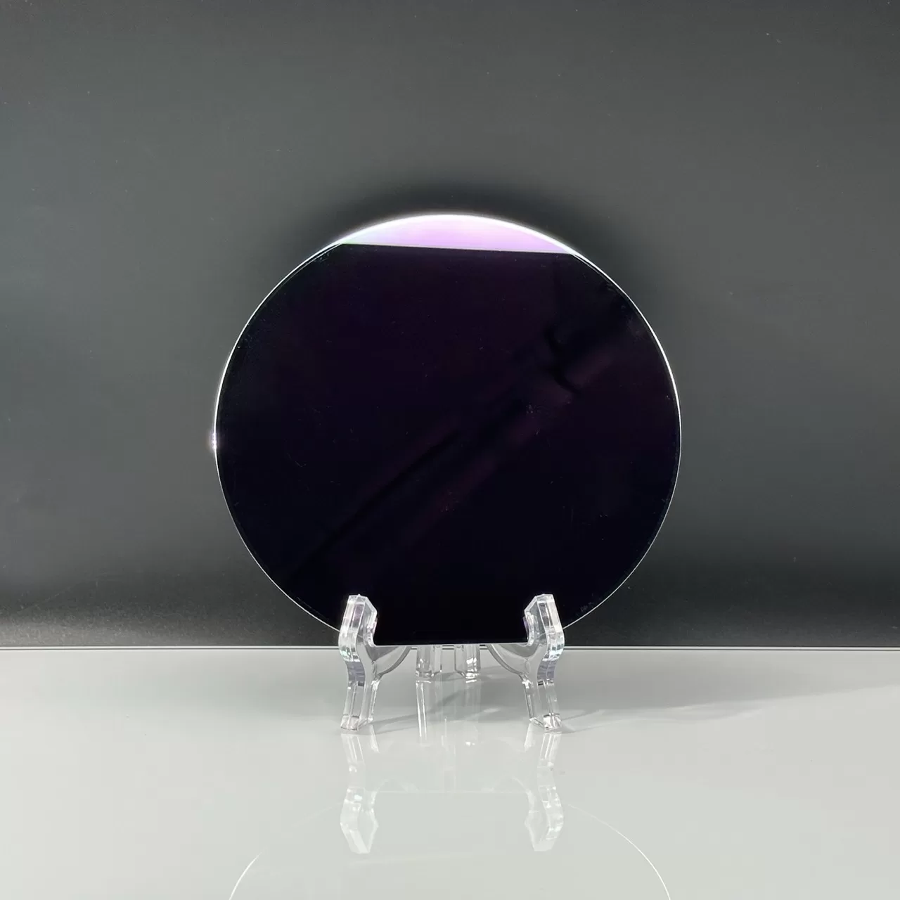
Micro-Electro-Mechanical Systems (MEMS) have revolutionized modern technology, enabling miniaturized sensors, actuators, and devices used in automotive, medical, consumer electronics, and aerospace industries. At the core of MEMS technology lies the silicon wafer, serving as a precisely engineered substrate for microfabrication.
Silicon wafers are favored for MEMS due to their excellent mechanical properties, high chemical stability, and compatibility with standard semiconductor fabrication processes. This article provides a comprehensive overview of silicon wafers for MEMS, including material properties, wafer types, fabrication methods, and application considerations.
Material Properties of Silicon Wafers
Silicon is a crystalline semiconductor with a diamond cubic crystal structure that provides unique advantages for MEMS fabrication:
- Mechanical Strength: High Young’s modulus (~130–185 GPa for single-crystal silicon) ensures rigidity and dimensional stability.
- Thermal Stability: Silicon withstands temperatures up to 1000°C, making it suitable for high-temperature processing steps such as oxidation, diffusion, and chemical vapor deposition.
- Chemical Compatibility: Resistant to most wet and dry etchants used in MEMS fabrication, allowing precise microstructuring.
- Electrical Properties: Doping allows silicon to be tailored for conductive or insulating regions, enabling integrated sensor or actuator designs.
Types of Silicon Wafers for MEMS
MEMS devices require wafers with different specifications depending on device geometry, mechanical requirements, and processing conditions:
- Single-Crystal Silicon (Monocrystalline) Wafers
- Most common type for MEMS due to uniform mechanical properties and minimal defects.
- Typically available in 100, 110, or 111 crystal orientations, influencing etching behavior and device performance.
- Polycrystalline (Multicrystalline) Silicon Wafers
- Less expensive, with smaller grain size and slightly lower mechanical uniformity.
- Used primarily in MEMS energy harvesters or sensors where ultra-high precision is not critical.
- Silicon-on-Insulator (SOI) Wafers
- Consist of a thin silicon device layer on a buried oxide (BOX) layer, atop a silicon handle wafer.
- SOI wafers are ideal for high-aspect-ratio MEMS structures, microfluidics, and precision sensors.
- Enable precise etch depth control and improved electrical isolation.
Wafer Fabrication for MEMS Applications
The production of silicon wafers suitable for MEMS involves several critical steps:
- Crystal Growth
- Czochralski (CZ) method: Produces high-quality monocrystalline silicon wafers with controlled resistivity.
- Float Zone (FZ) method: Produces ultra-pure silicon with minimal oxygen, suitable for high-performance MEMS devices.
- Wafer Slicing and Polishing
- Silicon ingots are sliced into wafers using wire saws, then lapped and polished to achieve sub-micron flatness and surface roughness suitable for microfabrication.
- Cleaning and Surface Preparation
- Wafers undergo rigorous RCA cleaning to remove organic, ionic, and particulate contaminants, ensuring optimal adhesion for thin films and photolithography masks.
- Doping and Oxidation (Optional)
- Wafers can be doped with boron, phosphorus, or arsenic to achieve desired electrical conductivity.
- Thermal oxidation can create SiO₂ layers for insulation, masking, or structural purposes.
Applications of Silicon Wafers in MEMS
Silicon wafers enable a wide range of MEMS devices:
- Sensors: Accelerometers, gyroscopes, pressure sensors, and bioMEMS devices.
- Actuators: Micro-mirrors, micro-pumps, and micro-valves for optical and fluidic systems.
- Microfluidics: Channels and reservoirs fabricated for lab-on-chip applications.
- Energy Harvesting: Piezoelectric and electrostatic microgenerators.
The crystal orientation, wafer thickness, and doping profile play critical roles in determining device performance, sensitivity, and reliability.
Choosing the Right Silicon Wafer for MEMS
Key considerations when selecting silicon wafers for MEMS include:
- Crystal Orientation: Influences etch rates and mechanical behavior of MEMS structures.
- Wafer Thickness: Thicker wafers provide structural rigidity; thinner wafers enable flexible or high-aspect-ratio structures.
- Doping and Resistivity: Tailor electrical properties for integrated circuits or sensing elements.
- Surface Quality: Flatness and roughness affect thin-film deposition, bonding, and optical performance.
- SOI vs Bulk Silicon: SOI wafers are preferred for high-precision devices with complex topographies.
Conclusion
Silicon wafers are the fundamental substrate for MEMS, combining mechanical strength, thermal stability, chemical resistance, and electrical tunability.
By selecting the appropriate wafer type, thickness, crystal orientation, and surface preparation, engineers can ensure high device yield, performance consistency, and long-term reliability in MEMS devices.
Advances in wafer technology, including SOI and high-purity monocrystalline silicon, continue to expand the capabilities of MEMS, enabling miniaturized sensors and actuators for increasingly complex applications across industrial, medical, and consumer markets.