
300mm vs. 200mm SiC Wafer Cost Analysis: At What Production Volume is the 12-Inch Transition Profitable?
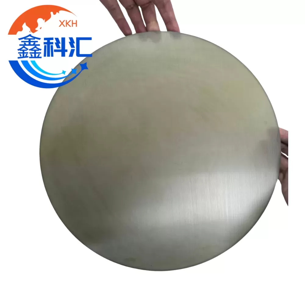
Silicon carbide (SiC) wafers have become a critical material for high-power electronics, electric vehicles, and advanced semiconductor devices. As the demand for higher efficiency, smaller form-factor devices grows, semiconductor manufacturers face a strategic decision: whether to transition from conventional 200mm (8-inch) SiC wafers to 300mm (12-inch) wafers. While larger wafers promise cost savings per device, […]
300mm SiC Wafers Challenges: The Technical Hurdles of Crystal Growth in Larger Diameters (EFG vs. PVT)
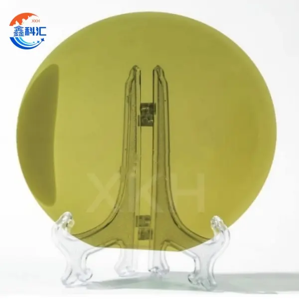
Silicon carbide (SiC) has emerged as a cornerstone material for high-power electronics, electric vehicles, and next-generation semiconductor devices due to its exceptional thermal conductivity, high breakdown voltage, and chemical stability. As the semiconductor industry pushes for larger wafer diameters to reduce production costs and increase throughput, the transition from conventional 150mm and 200mm SiC wafers […]
What to Look for in a SiC Wafer Technical Datasheet: A Modern Guide for Engineers and Researchers

Silicon carbide (SiC) has emerged as a cornerstone material in high-power electronics, high-frequency devices, and harsh-environment applications. Its superior thermal conductivity, high breakdown voltage, and chemical robustness make it indispensable in modern semiconductor technologies. However, leveraging SiC’s full potential begins long before fabrication—it starts with the wafer. Understanding a SiC wafer technical datasheet is therefore […]