
Silicon carbide (SiC) wafers have become a critical material for high-power electronics, electric vehicles, and advanced semiconductor devices. As the demand for higher efficiency, smaller form-factor devices grows, semiconductor manufacturers face a strategic decision: whether to transition from conventional 200mm (8-inch) SiC wafers to 300mm (12-inch) wafers. While larger wafers promise cost savings per device, the shift involves significant capital investment, technical challenges, and operational adjustments. Understanding the economic and technical trade-offs is essential for engineers, production managers, and procurement teams.
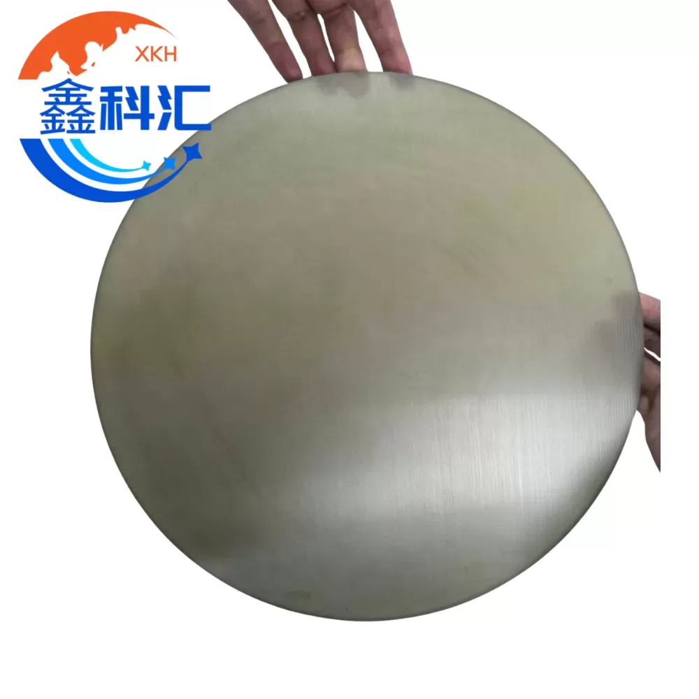
Why Consider 300mm SiC Wafers?
The primary motivation for scaling to 300mm wafers is cost efficiency. Larger wafers allow more die per wafer, reducing the cost per device. Additionally, 12-inch wafers are compatible with high-volume semiconductor production lines, improving throughput and enabling better integration with modern IC fabrication equipment.
Other benefits of transitioning include:
- Reduced handling and processing overhead: Fewer wafers are needed to achieve the same number of dies.
- Improved yield scalability: Advanced process control can reduce defect impact across more devices.
- Alignment with future device trends: High-power and EV applications increasingly demand large, high-quality wafers for devices such as MOSFETs, IGBTs, and Schottky diodes.
However, these benefits come at the cost of higher capital expenditure (CAPEX) and potentially higher operational complexity, which must be carefully evaluated.
Cost Structure Comparison: 200mm vs. 300mm Wafers
The economics of wafer scaling depend on several factors:
- Crystal Growth and Wafer Fabrication
- 200mm wafers: Well-established PVT or EFG processes, mature yield rates, lower defect density per wafer.
- 300mm wafers: Requires redesigned crystal growth reactors, stricter thermal gradient control, and longer growth times, increasing per-wafer cost.
- Processing Equipment Compatibility
- Larger wafers may require modified or new equipment for epitaxial growth, polishing, dicing, and packaging.
- Capital costs for a 300mm line can be 2–3x higher than a 200mm line, depending on automation and throughput.
- Yield Considerations
- Larger wafers have a higher probability of defects affecting the final die.
- Achieving low defect density (<1 cm^-2) is critical to ensure that the per-device cost advantage is realized.
- Operational Costs (OPEX)
- Energy consumption, gas usage, and maintenance costs increase with wafer size.
- Staff training and process optimization add indirect operational costs.
Cost per Die Analysis
Let’s consider a simplified scenario:
| Parameter | 200mm Wafer | 300mm Wafer |
|---|---|---|
| Wafer area | 31,400 mm² | 70,700 mm² |
| Die size | 50 mm² | 50 mm² |
| Dies per wafer (ideal) | 628 | 1,414 |
| Wafer cost | $4,000 | $10,000 |
| Defect impact | 5% | 8% |
| Effective dies per wafer | 597 | 1,300 |
| Cost per die | ~$6.70 | ~$7.70 |
Observation: At low volumes, 300mm wafers may not be cost-effective due to higher CAPEX and OPEX. However, as production volume increases, the per-die cost advantage emerges because fewer wafers are needed, reducing handling, cleaning, and processing overhead.
Production Volume Threshold for Profitability
The break-even point depends on several factors:
- Wafer cost differential: Higher 300mm wafer cost requires sufficient throughput to amortize CAPEX.
- Yield optimization: Efficient defect control is critical. A 10% higher defect rate on larger wafers can offset cost benefits.
- Equipment utilization: Maximizing reactor uptime and process efficiency ensures economies of scale.
Industry analyses suggest that for SiC power electronics, the 12-inch transition becomes profitable at production volumes exceeding 50,000–100,000 wafers per year, assuming defect densities are controlled and process efficiency is optimized.
Technical Challenges Impacting Cost
Transitioning to 300mm SiC wafers is not purely economic; technical hurdles also affect profitability:
- Thermal Stress Management: Larger wafers are more susceptible to bowing and cracking. Reactor design must mitigate thermal gradients to maintain flatness and uniformity.
- Epitaxial Layer Uniformity: Maintaining consistent EPI layer thickness and doping across 12-inch wafers is more challenging than with 200mm wafers.
- Crystal Growth Duration: Growth time for 300mm wafers is longer, affecting throughput. Optimization of PVT or EFG processes is essential.
Overcoming these challenges may require R&D investment and pilot production, further influencing the break-even point.
Strategic Considerations for Manufacturers
For companies evaluating the transition, several strategic points should guide decision-making:
- Align wafer size with market demand: If clients require high-volume EV or industrial power devices, 300mm wafers offer long-term advantages.
- Invest in process optimization: Focus on yield improvement, defect reduction, and uniformity to realize per-die cost benefits.
- Consider phased adoption: Hybrid production lines maintaining both 200mm and 300mm wafers allow gradual scaling while managing risk.
- Leverage automation and monitoring: Real-time process control reduces operational variability and ensures quality across larger wafers.
Conclusion
While 300mm SiC wafers promise significant cost savings per die and improved throughput, achieving profitability requires careful consideration of production volume, defect management, and equipment investment. Companies that master the technical and operational challenges of 12-inch SiC wafers will be positioned as leaders in the high-power electronics and EV markets, gaining both economic and technological advantages.
Ultimately, the transition is not just a matter of wafer size, but of strategic planning, process control, and production efficiency. Decision-makers must balance CAPEX, OPEX, yield, and market demand to determine the optimal point for adopting 300mm SiC wafer technology.