
Large-Area 12-Inch Silicon Carbide (SiC) Substrates: Advancing AR Optical Waveguides
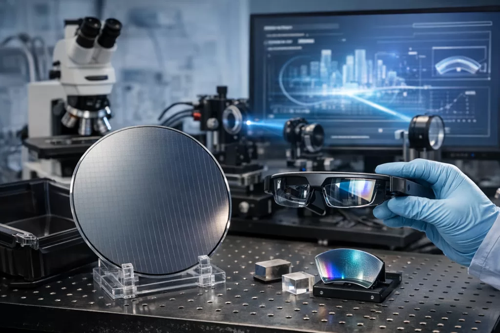
Recently, large-area 12-inch silicon carbide (SiC) substrates have emerged as a promising solution, providing an unprecedented combination of material properties suitable for next-generation AR devices.Augmented Reality (AR) technology is rapidly evolving, driven by higher demands for immersive displays, compact devices, and advanced optical performance. A key component enabling AR experiences is the optical waveguide, which […]
Technical Breakthrough and Industry Prospects of 14-Inch SiC Substrates

Silicon carbide (SiC), a third-generation semiconductor material, has attracted significant attention due to its wide bandgap, high breakdown electric field, and superior thermal conductivity. These properties make SiC a critical material for high-power electronic devices in electric vehicles (EVs), data centers, renewable energy systems, and other high-performance applications. In recent years, the wafer size of […]
SiC Wafers in High-Frequency Applications: Benefits and Practical Limitations
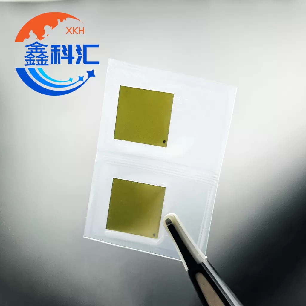
Silicon carbide (SiC) wafers have rapidly gained attention in high-frequency and high-power electronics due to their superior material properties compared to conventional silicon (Si). With a combination of wide bandgap, high thermal conductivity, and high breakdown electric field, SiC substrates provide performance advantages for RF devices, microwave transceivers, and high-speed power electronics. While these advantages […]
Understanding SiC Covalent Networks: The Backbone of a High-Performance Material
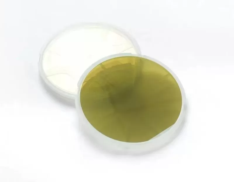
Silicon carbide (SiC) has emerged as one of the most important materials in modern electronics, power devices, and advanced ceramics. Its remarkable mechanical, thermal, and electrical properties stem from a unique feature at the atomic level: its covalent network structure. Understanding this network is key to appreciating why SiC performs so well in extreme conditions. […]