
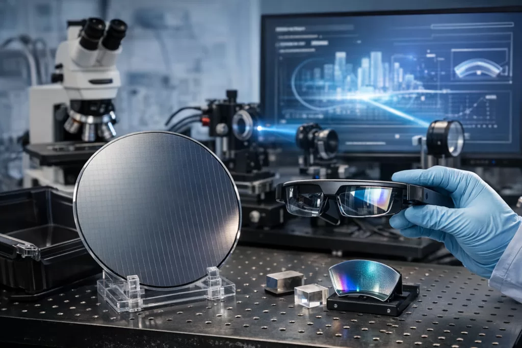
Recently, large-area 12-inch silicon carbide (SiC) substrates have emerged as a promising solution, providing an unprecedented combination of material properties suitable for next-generation AR devices.Augmented Reality (AR) technology is rapidly evolving, driven by higher demands for immersive displays, compact devices, and advanced optical performance. A key component enabling AR experiences is the optical waveguide, which channels light from microdisplays into the user’s eyes while preserving image clarity, brightness, and color fidelity. The performance of these waveguides heavily depends on the substrate material, which must meet strict requirements in optical transparency, thermal management, mechanical stability, and scalability.
Challenges of Conventional Substrates in AR
Traditional optical waveguides often utilize silicon or fused silica substrates. While these materials offer acceptable optical transparency, they encounter significant limitations in advanced AR applications:
- Thermal Limitations: High-brightness microdisplays generate substantial heat during operation. Silicon’s thermal conductivity (~150 W/m·K) is insufficient for effectively dissipating localized heat, which can cause image distortions, brightness non-uniformity, and potential long-term degradation of optical components.
- Mechanical Constraints: Large-area substrates are prone to warping, cracking, or deformation due to low hardness and relatively high thermal expansion of silicon or glass. This restricts the design and scale of AR waveguides, limiting the achievable field-of-view and device size.
- Manufacturing Efficiency: Large-area waveguides require uniform material quality with minimal defects. Traditional wafers often have a limited usable area, reducing yield and increasing production costs for high-performance AR modules.
Advantages of Silicon Carbide for AR Waveguides
Silicon carbide offers a unique combination of optical, thermal, and mechanical properties that address the limitations of conventional substrates:
- High Optical Transparency: High-purity SiC transmits visible light efficiently, minimizing optical loss in waveguides. This ensures sharp image projection and accurate color rendering for AR displays.
- Exceptional Thermal Conductivity: With a thermal conductivity ranging from 370 to 490 W/m·K, SiC effectively disperses heat in both lateral and vertical directions. This allows AR waveguides to maintain consistent optical performance, even under high-brightness microdisplay operation.
- Mechanical Robustness: SiC is extremely hard and strong, supporting large-area waveguides without warping or fracturing. Its low thermal expansion coefficient ensures dimensional stability during temperature variations, preserving the optical alignment and uniformity of waveguides.
- Electrical Insulation and Integration: SiC’s high resistivity and dielectric strength facilitate high-density integration of optical and electronic components within the same module. This enables complex multilayer waveguide structures with minimal electrical interference and high signal fidelity.
Why 12-Inch SiC Wafers Matter
Scaling to 12-inch SiC wafers represents a significant breakthrough for AR optical waveguides. Larger wafers offer several advantages:
- Increased Usable Area: A 12-inch wafer provides over twice the area of an 8-inch wafer, allowing multiple large waveguides to be fabricated simultaneously. This reduces material waste, improves yield, and lowers production costs.
- Compatibility with Existing Fabrication Lines: Many semiconductor and optical manufacturing processes are optimized for 12-inch wafers, including lithography, etching, and deposition. Using 12-inch SiC allows AR waveguide production to leverage existing infrastructure, avoiding costly retooling.
- Enabling Large-Scale AR Modules: Advanced AR devices require waveguides exceeding 100 mm × 100 mm for wider field-of-view or multi-display integration. 12-inch wafers provide sufficient area to fabricate these large modules in a single piece, simplifying assembly and improving optical consistency.
Industrial Potential and Early Applications
Early implementations of large-area SiC substrates in AR have demonstrated significant improvements in thermal management, mechanical stability, and optical clarity. Prototype AR waveguides using 12-inch SiC wafers have shown uniform light propagation, high brightness retention, and reduced warping under operational thermal loads. As AR devices continue to demand larger waveguides, higher brightness, and more compact integration, the use of 12-inch SiC substrates is expected to accelerate.
Beyond waveguides, these substrates could enable multifunctional optical components, including integrated diffractive optics, lenses, and thermal management layers, all fabricated on a single wafer-scale platform. This wafer-level integration enhances manufacturing efficiency, reduces assembly complexity, and ensures superior device performance.
Conclusion
Large-area 12-inch SiC substrates are poised to become a cornerstone material for next-generation AR optical devices. By combining excellent optical transparency, thermal conductivity, and mechanical strength with compatibility to existing wafer-scale fabrication infrastructure, SiC overcomes the critical challenges limiting conventional substrates. Early demonstrations in AR waveguides suggest that 12-inch SiC can significantly enhance optical performance, thermal stability, and manufacturability.
As the AR industry grows, the adoption of large-area SiC substrates will likely expand, supporting higher-brightness displays, larger field-of-view modules, and complex multilayer optical designs. This convergence of material performance and industrial scalability positions 12-inch SiC as a transformative technology for high-performance, manufacturable AR devices.