
Laser Stealth Dicing of SiC Wafers: Subsurface Microcracks, Edge Chipping, Dicing Quality, Inspection and Yield Control
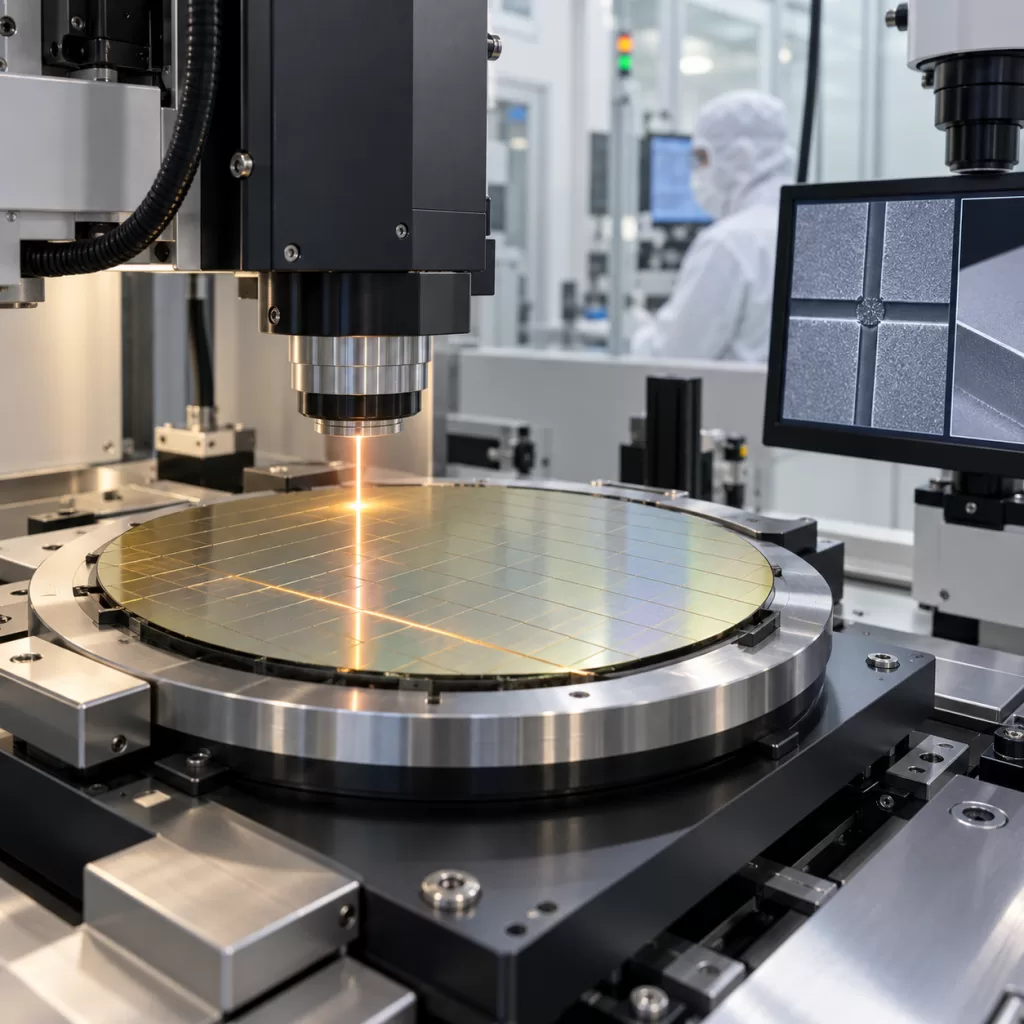
Silicon carbide wafers are increasingly used in high-power and high-temperature semiconductor devices, but they also present major challenges during singulation. Because SiC is extremely hard and brittle, conventional blade dicing can cause edge chipping, kerf loss, mechanical stress and tool wear. As device structures become smaller and wafer value increases, manufacturers are paying more attention […]
Common Defects in SiC Wafer and Their Impact on Device Performance
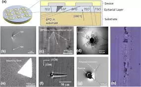
Silicon Carbide (SiC), as a third-generation wide-bandgap semiconductor material, has gained significant importance in power electronics, including electric vehicles, photovoltaic inverters, high-voltage power supplies, and industrial energy systems. Thanks to its wide bandgap, high breakdown electric field, and excellent thermal conductivity, SiC enables devices with higher efficiency, higher switching speed, and better high-temperature stability compared […]
The Manufacturing Process of Single Crystal Silicon Wafers
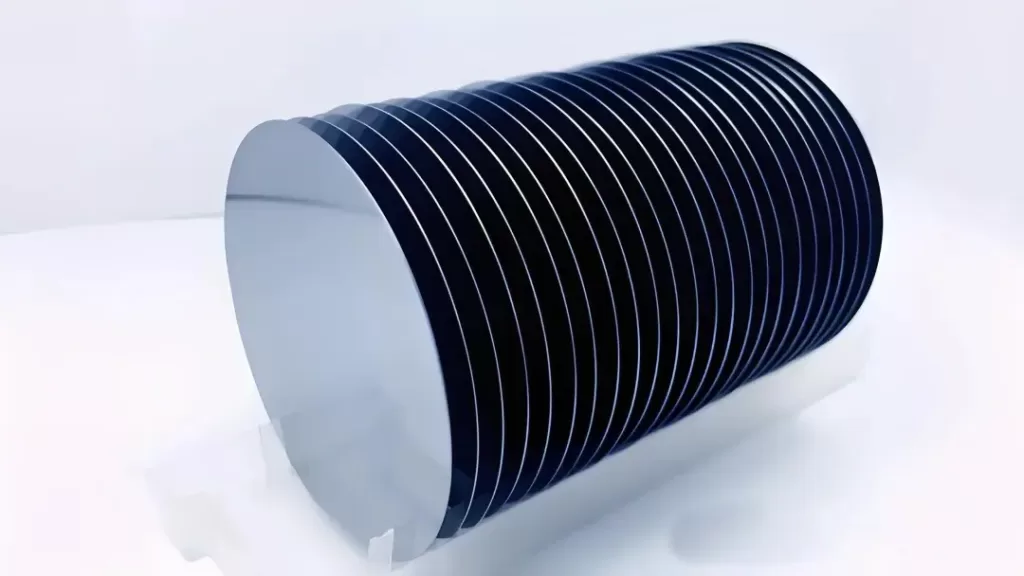
Silicon wafers are essential components in modern electronics, serving as the foundation for devices ranging from smartphones and computers to solar panels and semiconductor devices. The manufacturing of these wafers involves a series of highly precise steps, beginning with the creation of a single crystal silicon ingot and ending with the production of polished wafers […]