
Silicon carbide wafers are increasingly used in high-power and high-temperature semiconductor devices, but they also present major challenges during singulation. Because SiC is extremely hard and brittle, conventional blade dicing can cause edge chipping, kerf loss, mechanical stress and tool wear. As device structures become smaller and wafer value increases, manufacturers are paying more attention to dicing methods that can reduce damage and improve yield.
Laser stealth dicing has emerged as an important option for SiC wafer singulation. Instead of cutting completely through the wafer from the surface like a blade, stealth dicing focuses laser energy inside the wafer to form a modified internal layer. The wafer is then separated along that weakened plane. In principle, this method can reduce surface debris, lower kerf loss and improve throughput. However, for SiC wafers, dicing quality still depends heavily on controlling subsurface microcracks, edge chipping and process stability.
This article explains how laser stealth dicing works for SiC wafers, what defect risks must be controlled, how to inspect dicing quality, and what buyers should clarify when discussing SiC wafer dicing requirements with a supplier or processing partner.
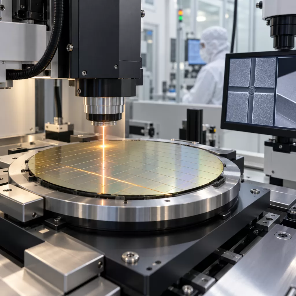
Why SiC Wafers Are Difficult to Dice
SiC offers excellent hardness, thermal conductivity, breakdown field and chemical stability, which are why it is used in advanced power devices. But these same material characteristics also make dicing more difficult.
Common challenges include:
- high hardness and brittleness;
- strong resistance to mechanical cutting;
- risk of edge chipping;
- subsurface crack propagation;
- sensitivity to stress concentration;
- tighter die-edge quality requirements;
- increasing wafer value and yield pressure.
When a blade cuts SiC, mechanical contact can easily generate edge defects. These defects may not only reduce die strength, but can also become failure initiation sites during packaging or device operation. That is why many manufacturers evaluate laser-based processes as an alternative.
What Is Laser Stealth Dicing?
Laser stealth dicing is a process in which a focused laser beam is directed into the interior of the wafer rather than only acting on the surface. The laser creates a modified layer or internal damage region at a controlled depth. After laser scanning, external force or expansion can separate the wafer along the processed lines.
Compared with conventional blade dicing, stealth dicing offers several potential advantages:
- reduced kerf loss;
- less tool wear;
- lower particle generation on the wafer surface;
- narrower streets for higher die density;
- lower mechanical contact during cutting;
- improved productivity in some applications.
For SiC wafers, however, success depends on whether the internal modified layer is stable and whether crack propagation remains controllable.
Why Subsurface Microcracks Matter
Subsurface microcracks are one of the most important concerns in laser stealth dicing of SiC wafers.
Because the laser energy is intentionally focused inside the wafer, the process relies on localized structural change. If this internal modification is too strong, too deep or non-uniform, it can generate uncontrolled microcracks. If it is too weak, the wafer may not separate cleanly, or higher separation force may be required later.
Subsurface microcracks matter because they can lead to:
- reduced die strength;
- uncontrolled crack extension;
- rough fracture surfaces;
- hidden reliability risks;
- die-edge weakness during assembly;
- yield loss during separation or pick-up.
Unlike large surface chips that are easy to see, subsurface cracks may remain partially hidden until later inspection or packaging. This makes process control and inspection especially important.
Edge Chipping Is Still a Major Risk
Even though stealth dicing reduces direct blade contact, edge chipping can still occur.
Possible causes include:
- improper laser focus depth;
- excessive local stress near the dicing street;
- non-optimized pulse energy;
- weak wafer support;
- poor tape or frame mounting;
- unstable wafer thickness;
- high separation force after laser processing;
- pre-existing edge defects or backside damage.
For high-value SiC die, edge chipping is not only a cosmetic issue. It can influence die strength, package reliability and downstream yield. Large or irregular chips can also affect die attach, wire bonding clearance or sealing performance depending on the device design.
That is why buyers should not assume that “laser dicing” automatically means “no edge damage.” Real quality depends on the actual process window.
Key Factors That Influence Stealth Dicing Quality
1. Wafer Thickness
Wafer thickness strongly affects laser focus strategy and separation behavior.
A thicker wafer may require different focal-depth control and scan conditions. A thinner wafer may be more vulnerable to bow, local deformation and crack propagation. For thinned SiC wafers, support conditions during dicing also become more critical.
2. Laser Parameters
Important laser-related factors include:
- wavelength;
- pulse width;
- pulse energy;
- repetition rate;
- focus position;
- scan speed;
- number of passes;
- line pitch.
If energy is too high, the modified layer may become excessive and generate uncontrolled cracking. If energy is too low, separation may become incomplete or inconsistent.
3. Wafer Mounting and Support
SiC wafers are typically mounted on dicing tape and ring frames. If the tape tension is not uniform, or if the frame is not flat, additional stress may be introduced before or during separation.
Poor support can contribute to:
- non-uniform crack propagation;
- variation in street quality;
- local chipping;
- die movement;
- breakage during expansion.
4. Street Design and Die Size
Dicing street width, die size and die layout also affect outcomes. Very narrow streets reduce available tolerance. Small die or complex layouts may require tighter process control to maintain clean separation.
5. Incoming Wafer Quality
Laser stealth dicing cannot fully compensate for poor incoming wafer condition. If the wafer already has:
- edge chips;
- backside grinding damage;
- excessive bow or warp;
- surface particles;
- thickness variation;
- residual stress,
then dicing quality may become less stable.
Common Defects in Laser Stealth Dicing of SiC Wafers
When evaluating dicing results, manufacturers should watch for several typical defect modes:
Subsurface Microcracks
Hidden or partially hidden cracks below the surface, often caused by excessive or uneven internal modification.
Edge Chipping
Material loss along the die edge or wafer street, often seen after separation.
Incomplete Separation
The modified layer forms, but the die does not separate cleanly, requiring excessive external force.
Rough Sidewalls or Fracture Faces
The die edge may look irregular, affecting mechanical integrity and appearance.
Surface Burn or Thermal Damage
Although stealth dicing is designed to limit surface damage, poor parameter control can still create visible heat effects or local discoloration.
Particle Contamination
Fracture residue, broken fragments or tape contamination can affect the wafer and downstream assembly.
How to Inspect Dicing Quality
Inspection is essential because not all defects are visible with the naked eye.
Typical inspection methods may include:
- optical microscope inspection for visible chipping and street condition;
- edge inspection at higher magnification;
- surface particle inspection;
- cross-section analysis for crack depth and fracture profile;
- thickness and bow/warp measurement before dicing;
- infrared or other internal-defect observation methods where applicable;
- die strength or breakage testing;
- sampling inspection after separation.
For production control, manufacturers often focus on several practical quality indicators:
- maximum allowable edge chip size;
- presence or absence of subsurface crack extension;
- die separation completeness;
- sidewall quality;
- particle level;
- final die yield.
If the application is high reliability, buyers may also request tighter internal inspection or reliability sampling.
Yield Control in SiC Stealth Dicing
Yield control should not be limited to the dicing tool itself. It should cover the full process flow, including:
- incoming wafer inspection;
- backside condition after grinding;
- tape and frame qualification;
- laser process optimization;
- separation force control;
- post-dicing inspection;
- die handling and packaging.
A stable stealth dicing process typically depends on building a usable process window rather than relying on a single “best” setting. That means identifying the range of laser energy, scan speed, focus depth and mounting condition that consistently delivers acceptable quality.
For example, a process may appear acceptable on one wafer lot but become unstable when thickness, warp or incoming edge condition changes. True yield control requires evaluating variation, not only nominal results.
Laser Stealth Dicing vs Blade Dicing for SiC Wafers
Both methods have advantages, and the best choice depends on the wafer, die design and yield target.
Blade Dicing
Advantages:
- mature and widely used;
- easier for some conventional layouts;
- familiar process flow.
Limitations:
- blade wear when cutting hard SiC;
- mechanical stress;
- larger kerf loss;
- higher risk of surface chipping and debris.
Laser Stealth Dicing
Advantages:
- reduced direct mechanical contact;
- potential for smaller kerf loss;
- useful for high-density layouts;
- reduced consumable wear in some cases.
Limitations:
- requires precise process tuning;
- subsurface microcracks must be controlled;
- separation stability can vary with wafer condition;
- inspection becomes even more important.
For many buyers, the most important question is not which method is “better” in theory, but which method can provide stable yield for their actual wafer design and die requirements.
What Buyers Should Clarify with a Supplier
When discussing SiC wafer dicing services or custom wafer preparation, it is helpful to define the following:
| Item | Information to Confirm |
|---|---|
| Wafer diameter | 2 inch, 4 inch, 6 inch, 8 inch |
| Polytype | 4H-SiC or other |
| Wafer thickness | starting and final thickness |
| Surface condition | polished face, backside condition |
| Bow / warp | allowable limits |
| Die size | target chip dimensions |
| Street width | available dicing lane |
| Dicing method | stealth dicing / blade dicing / laser ablation |
| Edge quality | acceptable chip size or crack level |
| Inspection standard | optical, crack inspection, sampling plan |
| Mounting | tape type and ring frame specification |
| Shipment format | full wafer, frame-mounted wafer, singulated die |
The clearer the specification, the easier it is to match the wafer, dicing process and inspection method to the end use.
Conclusion
Laser stealth dicing is a promising technology for SiC wafer singulation, especially where reduced kerf loss, lower mechanical contact and improved die density are important. However, the process is not automatically defect-free. Subsurface microcracks, edge chipping, incomplete separation and hidden damage can still affect dicing quality and yield if the process is not well controlled.
For SiC wafers, successful stealth dicing depends on the interaction between wafer thickness, incoming quality, laser parameters, tape mounting, separation method and inspection criteria.
If you are sourcing SiC wafers for device fabrication, or if you require custom dicing support, it is important to discuss not only wafer size and thickness, but also die layout, edge-quality expectations, crack control and post-dicing inspection requirements.
ZMSH can support custom SiC wafer requirements for semiconductor processing, including substrate supply, thickness specification and technical communication for downstream dicing and handling applications.