
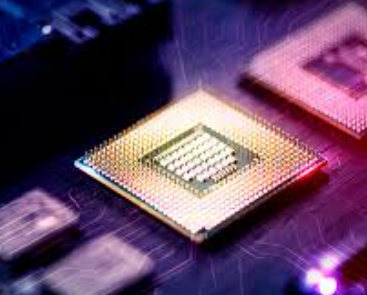
silicon wafer ‘s abstract
Silicon wafers are fundamental substrates in semiconductor manufacturing, crucial for the fabrication of integrated circuits and electronic devices. This abstract focuses on prime silicon wafers suitable for both P-type and N-type semiconductor applications, ranging in diameter from 2 inches to 12 inches. The properties and characteristics of these wafers play a pivotal role in determining the performance and efficiency of semiconductor devices. This abstract provides an overview of the specifications, quality standards, and applications of silicon wafers in contemporary semiconductor technology, emphasizing their significance in the production of advanced electronic components.
silicon wafer ‘s properties
The properties of silicon wafers, used extensively in semiconductor manufacturing, include:
- โครงสร้างผลึก: Silicon wafers typically have a crystalline structure, often single-crystal (monocrystalline) or polycrystalline, which affects their electrical and mechanical properties.
- คุณสมบัติทางไฟฟ้า: Silicon wafers are semiconductors with an intrinsic electrical resistivity that can be controlled through doping with specific elements (e.g., boron for P-type doping, phosphorus for N-type doping). This allows for the creation of diodes, transistors, and other electronic components.
- สมบัติทางกล: Silicon wafers are brittle and prone to breakage if mishandled, but they also have excellent flatness and surface uniformity, crucial for photolithography processes in semiconductor fabrication.
- สมบัติทางแสง: Silicon wafers are typically opaque in the visible spectrum but transparent in the infrared range, making them suitable for certain optoelectronic applications.
- คุณสมบัติทางความร้อน: Silicon has a relatively high thermal conductivity and can withstand high temperatures, making it suitable for applications where heat dissipation is critical.
- Chemical Properties: Silicon wafers are stable in most environments but can react with strong acids and bases. Surface passivation and doping techniques are used to improve chemical stability and performance in specific applications.
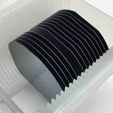
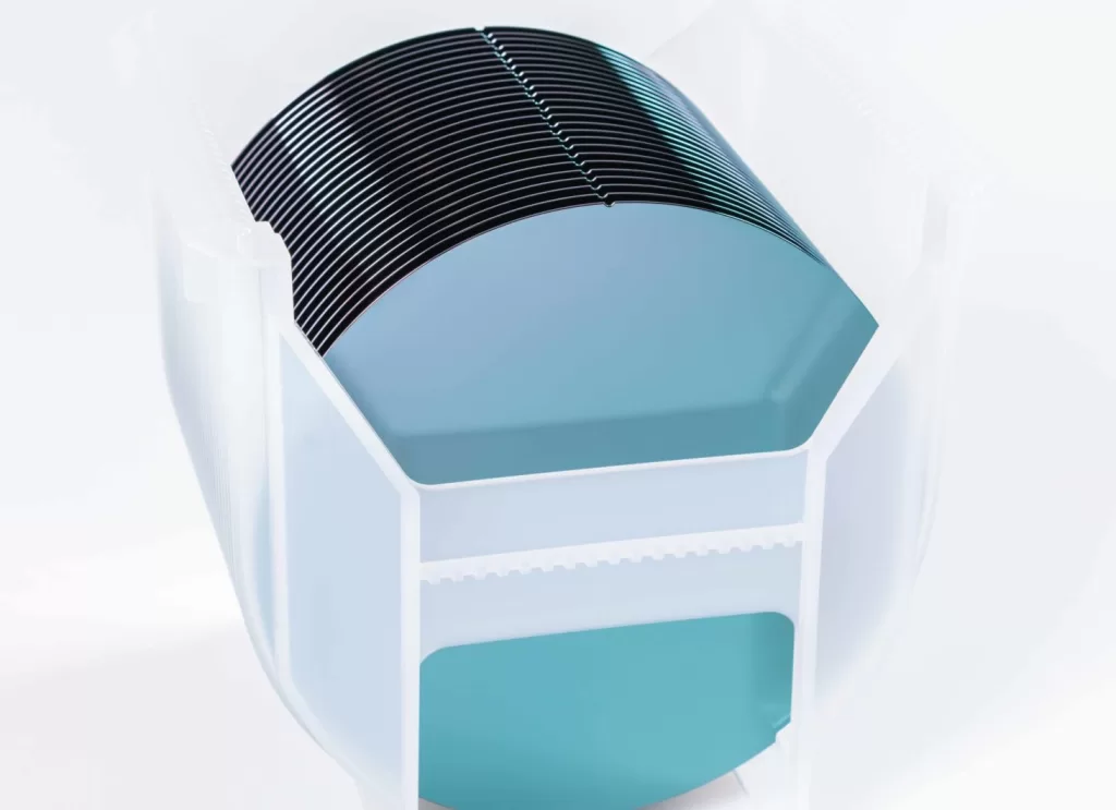
- Size and Thickness: Silicon wafers come in various sizes, commonly ranging from 2 inches to 12 inches in diameter, and thicknesses ranging from tens to hundreds of micrometers, depending on the application requirements.
These properties make silicon wafers indispensable in the production of integrated circuits, solar cells, MEMS devices, and various other semiconductor devices critical to modern technology.
silicon wafer’s application
Silicon wafers are extensively used in a variety of applications across several industries, primarily due to their unique properties as semiconductor substrates. Some key applications include:
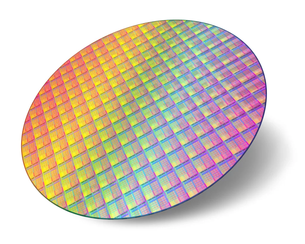
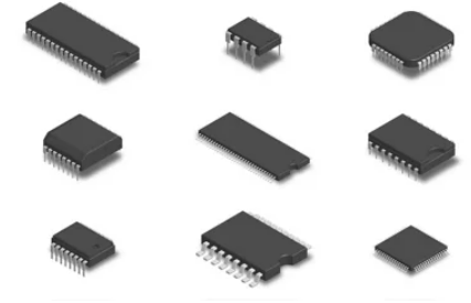
- Integrated Circuits (ICs): Silicon wafers form the foundational material for manufacturing integrated circuits (ICs) used in electronic devices such as computers, smartphones, and consumer electronics. The wafers are processed to create transistors, diodes, and other components essential for circuit functionality.
- Solar Cells: Silicon wafers are crucial for photovoltaic (PV) solar cells used in solar panels. These wafers are doped to create P-N junctions that convert sunlight into electricity efficiently. They are used both in monocrystalline and polycrystalline forms to meet various efficiency and cost requirements.
- MEMS (Microelectromechanical Systems): MEMS devices, which combine mechanical and electrical components on a silicon substrate, utilize them for their precise manufacturing processes. Applications include accelerometers, gyroscopes, pressure sensors, and microphones.
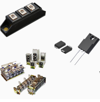
- อุปกรณ์ไฟฟ้า: They are used in power semiconductor devices such as MOSFETs (Metal-Oxide-Semiconductor Field-Effect Transistors) and IGBTs (Insulated Gate Bipolar Transistors). These devices are essential for controlling and switching electrical power efficiently in applications ranging from electric vehicles to industrial motor drives.
- Optoelectronics: They are used in optoelectronic devices such as photodiodes, LEDs (Light-Emitting Diodes), and optical sensors. Silicon-based photonic integrated circuits (PICs) are also gaining traction in telecommunications for data transmission and optical signal processing.
- Microelectronics and Nanotechnology: Silicon wafers serve as platforms for research and development in microelectronics and nanotechnology. They enable the fabrication of nanoscale structures and devices, contributing to advancements in quantum computing, biomedical sensors, and nanoelectronics.
- Wafer Level Packaging:They are integral to wafer-level packaging (WLP) processes, where multiple semiconductor devices are integrated and packaged directly on the wafer before being separated into individual components. This approach reduces packaging costs and enhances device performance.
Overall, silicon wafers play a critical role in enabling advancements across various technological fields, driving innovations in electronics, energy generation, sensing, and communications.

All questions and answers about silicon wafers.
What is a silicon wafer used for?
1. Integrated Circuits (ICs)
They are fundamental in the production of integrated circuits, which are the building blocks of most electronic devices.
- Microprocessors and CPUs: Central processing units in computers are fabricated on them.
- Memory Chips: DRAM, SRAM, and Flash memory used in computers, smartphones, and other electronic devices.
- ASICs and FPGAs: Application-specific integrated circuits and field-programmable gate arrays for specialized applications in telecommunications, automotive, and more.
- Analog Devices: Operational amplifiers, voltage regulators, and analog-to-digital converters.
2. Microelectromechanical Systems (MEMS)
MEMS devices combine electrical and mechanical components on a single silicon wafer.
- Accelerometers and Gyroscopes: Used in smartphones, gaming controllers, and automotive airbag systems.
- Pressure Sensors: Used in medical devices, automotive systems, and industrial applications.
- Inkjet Printer Heads: MEMS technology is used to precisely control the ejection of ink droplets.
3. Photovoltaic Cells
They are used to create photovoltaic cells, which convert sunlight into electricity.
- Monocrystalline Silicon Solar Cells: Made from a single continuous crystal structure, offering high efficiency.
- Polycrystalline Silicon Solar Cells: Made from silicon crystals melted together, generally less expensive but also less efficient.
- Thin-Film Solar Cells: Though not strictly made from wafers, thin-film technology often involves silicon materials and offers flexible application possibilities.
4. อุปกรณ์ไฟฟ้า
They are essential in the fabrication of devices that control and convert electrical power.
- Power MOSFETs and IGBTs: Used in power supplies, motor drives, and electric vehicles to efficiently switch and amplify electrical power.
- Rectifiers and Diodes: Convert AC to DC in power supplies for consumer electronics and industrial equipment.
5. Optoelectronics
Devices that convert electrical signals to optical signals and vice versa are often fabricated on silicon wafers.
- LEDs: Light-emitting diodes used in displays, lighting, and indicators.
- Photodetectors: Used in cameras, optical communication systems, and medical imaging.
- Laser Diodes: Used in fiber optic communications, barcode scanners, and laser pointers.
6. Sensors
They are used to create a variety of sensors for different applications.
- Temperature Sensors: Used in climate control systems, medical devices, and industrial processes.
- Biosensors: Used in medical diagnostics to detect biological molecules.
- Gas Sensors: Used in environmental monitoring and industrial safety.
7. Radio Frequency (RF) Devices
They are used to create devices that operate at radio frequencies.
- RFICs: Radio frequency integrated circuits used in wireless communication devices such as smartphones and Wi-Fi routers.
- MMICs: Monolithic microwave integrated circuits used in satellite communication and radar systems.
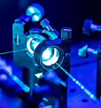
8. Photonics
Silicon photonics involves the use of silicon wafers to manipulate light for communication and signal processing.
- Optical Interconnects: Used in data centers and high-speed communication systems to transfer data with light.
- Waveguides and Modulators: Guide and modulate light signals for processing and communication purposes.
9. Quantum Computing
Silicon wafers are being explored for use in quantum computing, where quantum bits (qubits) can be created and manipulated on silicon substrates.
- Quantum Dots: Used to create qubits for quantum computing.
- Superconducting Circuits: Silicon wafers are used as substrates for superconducting materials in some quantum computing architectures.
10. Research and Development
Silicon wafers are used extensively in research to develop new materials, devices, and technologies.
- Nanotechnology: Research in nanoscale materials and devices often uses silicon wafers as substrates.
- วิทยาศาสตร์วัสดุ: Investigating new semiconductor materials and their properties.
Silicon wafers are vital in the electronics industry due to their versatility, availability, and the mature manufacturing infrastructure that exists to process and manipulate them.
What are 3 types of silicon wafers?
There are several types of silicon wafers, but three commonly referenced types include:
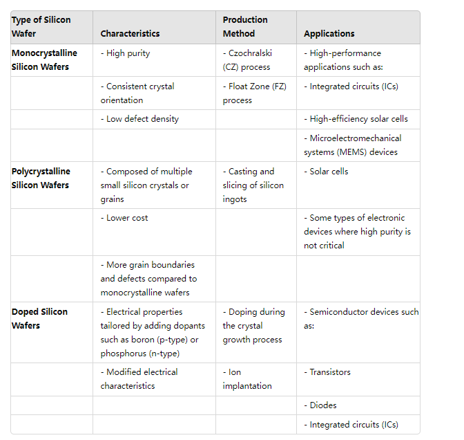
1. Monocrystalline Silicon Wafers
These wafers are made from a single continuous crystal structure and have a high level of purity and uniformity.
- Characteristics: High purity, consistent crystal orientation, and low defect density.
- Production Method: Czochralski (CZ) process or Float Zone (FZ) process.
- การประยุกต์ใช้: Used in high-performance applications such as integrated circuits, solar cells, and MEMS devices.
2. Polycrystalline Silicon Wafers
Also known as multicrystalline silicon wafers, these are composed of multiple small silicon crystals or grains.
- Characteristics: Lower cost, simpler manufacturing process, but with more grain boundaries and defects compared to monocrystalline wafers.
- Production Method: Casting and slicing of silicon ingots.
- การประยุกต์ใช้: Commonly used in solar cells and some types of electronic devices where high purity is not as critical.
3. Doped Silicon Wafers
These wafers have been intentionally infused with specific impurities (dopants) to alter their electrical properties.
- Characteristics: Can be tailored to have specific electrical characteristics by adding dopants such as boron (p-type) or phosphorus (n-type).
- Production Method: Doping during the crystal growth process or through ion implantation.
- การประยุกต์ใช้: Widely used in semiconductor devices such as transistors, diodes, and integrated circuits.
Each type of silicon wafer has its own unique properties and applications, making them suitable for different aspects of the electronics and solar industries.
here is a table summarizing the differences between monocrystalline silicon wafers, polycrystalline silicon wafers, and doped silicon wafers:
What is the difference between silicon and silicon wafer?
The terms “silicon” and “silicon wafer” refer to different forms and uses of the same chemical element, silicon (Si). Here’s a detailed explanation of their differences:
ซิลิคอน
- Nature: Silicon is a chemical element with the symbol Si and atomic number 14. It is a hard and brittle crystalline solid with a blue-grey metallic luster.
- Occurrence: It is the second most abundant element in the Earth’s crust, after oxygen. It is typically found in the form of compounds, such as silicon dioxide (sand) and silicates.
- Raw Form: In its natural state, silicon is not pure but combined with other elements.
- Uses: Silicon is used in various forms:
- Metallurgical Grade Silicon: Used in steelmaking, aluminum casting, and chemical processes.
- Silicon Dioxide (Silica): Used in glass making, ceramics, and as a raw material for producing pure silicon.
- Silicon Compounds: Used in various industrial applications, such as silicones in sealants, adhesives, and lubricants.
แผ่นซิลิคอนเวเฟอร์
- Nature: A silicon wafer is a thin slice of silicon crystal that has been carefully processed to have a very flat and smooth surface.
- การผลิต: Silicon wafers are produced through several steps:
- Purification: Raw silicon is purified to create semiconductor-grade silicon.
- การเจริญเติบโตของคริสตัล: A single crystal of silicon is grown using methods like the Czochralski (CZ) process or the Float Zone (FZ) process.
- Slicing: The crystal is sliced into thin wafers.
- Polishing and Etching: Wafers are polished and chemically etched to achieve the required surface flatness and cleanliness.
- Uses: Silicon wafers are specifically used in the semiconductor industry:
- Integrated Circuits (ICs): The foundation for manufacturing ICs, which are found in almost all electronic devices.
- Photovoltaic Cells: Used in solar panels to convert sunlight into electricity.
- Microelectromechanical Systems (MEMS): Used in sensors, actuators, and other microdevices.
- Other Semiconductor Devices: Includes transistors, diodes, and various types of sensors.
Key Differences
- Form: Silicon refers to the raw element or its various compounds and forms in nature, while a silicon wafer is a specifically processed and manufactured product.
- Purity: Silicon wafers are made from highly purified silicon suitable for electronic applications, whereas raw silicon may contain impurities and is used for more general purposes.
- การประยุกต์ใช้: Silicon wafers are used primarily in high-tech industries like electronics and solar energy, while raw silicon and its compounds are used in a broader range of industrial applications.
In summary, silicon is the basic element found in nature, while silicon wafers are highly processed and pure slices of silicon used mainly in the semiconductor industry for electronic device fabrication.
How are silicon wafers made into chips?
The process of making silicon wafers into chips (integrated circuits or ICs) involves several complex and highly controlled steps. Here’s a detailed overview of the process:
1. Design and Mask Preparation
- Circuit Design: Engineers design the circuit using specialized software, creating a detailed blueprint of the IC.
- Mask Creation: The design is then transferred onto a series of photomasks, which are templates that define the patterns to be transferred onto the silicon wafer. Each mask corresponds to a specific layer of the IC.
2. Silicon Wafer Preparation
- การเจริญเติบโตของคริสตัล: A single crystal of silicon is grown using methods like the Czochralski (CZ) process.
- Wafer Slicing: The silicon crystal is sliced into thin wafers using a diamond saw.
- Wafer Polishing and Cleaning: The wafers are polished to a mirror finish and cleaned to remove any contaminants.
3. Oxidation
- Thermal Oxidation: The wafer is heated in a furnace with oxygen or steam to grow a thin layer of silicon dioxide (SiO2) on its surface. This oxide layer acts as an insulator and a protective barrier.
4. Photolithography
- Photoresist Application: A light-sensitive photoresist material is applied to the wafer.
- Exposure: The wafer is exposed to ultraviolet (UV) light through a photomask, which transfers the mask’s pattern onto the photoresist.
- Development: The exposed photoresist is developed, revealing the pattern of the IC design on the wafer.
5. Etching
- Etching: The wafer undergoes etching processes (wet or dry) to remove the exposed areas of silicon dioxide or silicon, creating the desired pattern on the wafer surface.
6. Doping
- Ion Implantation or Diffusion: Dopants (such as boron or phosphorus) are introduced into the silicon to modify its electrical properties, creating p-type or n-type regions.
7. Deposition
- Chemical Vapor Deposition (CVD) or Physical Vapor Deposition (PVD): Thin films of various materials (such as metals for interconnects) are deposited onto the wafer to form different layers of the IC.
8. Planarization
- Chemical Mechanical Planarization (CMP): The wafer surface is polished to ensure a flat and smooth surface for subsequent layers.
9. Repeating Steps
- The steps of photolithography, etching, doping, and deposition are repeated multiple times to build up the multiple layers of the IC, including transistors, capacitors, and interconnects.
10. Metallization
- Interconnect Formation: Metal layers (usually aluminum or copper) are deposited and patterned to form the interconnections between different components of the IC.
11. Passivation
- Protective Layer: A final protective layer (such as silicon nitride or silicon dioxide) is deposited over the entire wafer to protect the ICs from contamination and damage.
12. Testing and Dicing
- Wafer Testing: The wafer is tested to identify functional and non-functional ICs.
- Dicing: The wafer is cut into individual chips using a diamond saw or laser.
13. บรรจุภัณฑ์
- Chip Packaging: Each individual chip is mounted into a protective package that provides electrical connections to the outside world and protects the chip from physical damage and contamination.
- Final Testing: The packaged chips undergo final testing to ensure they meet specifications.
14. Distribution
- The finished and tested chips are then shipped to customers or further integrated into electronic devices.
This entire process, from raw silicon to finished ICs, involves precision, advanced technology, and strict quality control to produce the highly complex and miniaturized electronic components used in modern devices.
What are the advantages of silicon wafer?
Silicon wafers offer several advantages, which have contributed significantly to their widespread use in various industries, especially in electronics and solar energy applications. Here are the key advantages:
- Semiconductor Properties: Silicon wafers are excellent semiconductors, meaning they can conduct electricity under some conditions and act as insulators under others. This property is fundamental for their use in electronic devices like integrated circuits (ICs), transistors, and diodes.
- Abundant Raw Material: Silicon is the second most abundant element in the Earth’s crust after oxygen. This abundance ensures a stable and consistent supply for manufacturing purposes, reducing dependency on scarce resources.
- High Purity: Silicon wafers can be manufactured with extremely high purity levels, essential for the production of reliable electronic components. Purification processes remove impurities to ensure consistent electrical and mechanical properties across wafers.
- Versatility: Silicon wafers can be tailored for specific applications by varying doping levels and surface treatments. This versatility allows for the production of a wide range of electronic devices, from microprocessors to solar cells to sensors.
- สมบัติทางกล: Silicon wafers exhibit mechanical strength and durability, allowing them to withstand various manufacturing processes such as polishing, etching, and deposition without deformation or cracking.
- Integration with Existing Technology: Silicon wafers are compatible with established semiconductor manufacturing processes and equipment. This compatibility streamlines production, reduces costs, and facilitates continuous technological advancements in the semiconductor industry.
- Miniaturization: Silicon wafers enable the fabrication of miniaturized electronic components due to their ability to form precise and intricate patterns at the nanoscale level. This capability supports the ongoing trend towards smaller and more efficient electronic devices.
- Cost-Effective Production: Despite the complex manufacturing processes involved, silicon wafer production benefits from economies of scale. Mass production and standardized processes contribute to lower per-unit costs, making silicon wafers economically viable for a wide range of applications.
- Reliability and Performance: Silicon wafers offer consistent electrical performance and reliability. This predictability is crucial for the performance and longevity of electronic devices, ensuring stable operation under varying conditions.
- Environmental Benefits: In the context of solar energy, silicon wafers are key components in photovoltaic cells used to generate renewable electricity. Solar panels made from silicon wafers contribute to reducing greenhouse gas emissions and reliance on fossil fuels.
These advantages collectively make silicon wafers indispensable in modern technology, playing a critical role in advancing electronics, renewable energy, telecommunications, and various other high-tech industries.