
Silicon Carbide (SiC) stands today as one of the most strategically important materials in advanced manufacturing and power electronics. It is widely used in electric vehicles, renewable energy systems, aerospace, and high-temperature industrial equipment. Yet its rise from a laboratory curiosity to a critical industrial material spans more than 130 years of scientific exploration and technological evolution. Understanding this journey helps reveal why SiC has become so essential to the future of energy and electronics.
1. The 19th Century: An Accidental Discovery Leads to a New Material
The story begins in 1891, when American scientist Edward Acheson attempted to create artificial diamonds. During experiments that involved heating clay and coke to extremely high temperatures, he unintentionally synthesized a new crystalline compound. This material demonstrated exceptional hardness, chemical stability, and heat resistance. Acheson named it Silicon Carbide and later commercialized it under the product name “Carborundum.”
At this early stage, SiC was valued almost exclusively as an industrial abrasive. Its properties made it an ideal material for grinding wheels, cutting tools, and polishing powders. While scientists noticed its unique crystalline structure, its electronic properties had not yet attracted significant attention.
2. Early 20th Century: Industrial Expansion and Ceramic Applications
As manufacturing expanded, SiC found new roles across high-temperature and corrosive industrial environments. Metallurgy, steelmaking, and chemical processing industries adopted SiC for furnace linings, heating elements, nozzles, bearings, and refractory components.
This period established the foundation for SiC as a robust ceramic material. However, the crystals produced were polycrystalline and impure, preventing any serious exploration of electronic applications. Researchers began documenting SiC’s polytypes—unique crystal structures that later became crucial for semiconductor research—but the material was still far from entering the electronics world.
3. Mid-20th Century: First Steps Toward Semiconductor Exploration
The growing interest in semiconductor physics after World War II opened new doors for SiC research. Scientists discovered that SiC had a wide bandgap, high thermal conductivity, and a high electric breakdown field. These features theoretically made it suitable for high-voltage, high-temperature, and high-frequency applications.
In the 1950s and 1960s, the first SiC-based electronic components were produced, such as early rectifiers and diodes. Although innovative for the time, the performance of these devices could not compete with silicon and germanium, which were easier to fabricate and purify.
The limitations were clear:
- Crystal defects were abundant
- Large, high-quality wafers were nearly impossible to grow
- Reliable doping and processing methods did not yet exist
As a result, SiC remained primarily a ceramic material throughout most of the 20th century.
4. Late 20th Century: Breakthroughs in Crystal Growth and Epitaxy
A defining shift occurred in the 1980s and 1990s. Researchers developed new processes that finally allowed SiC to reach semiconductor-grade purity.
Key breakthroughs included:
- PVT (Physical Vapor Transport) growth techniques that produced larger and more uniform SiC single crystals
- CVD (Chemical Vapor Deposition) epitaxy methods that enabled high-quality, low-defect SiC epitaxial layers
- Improvements in การฝังไอออน, dry etching, oxidation, และ interface engineering, enabling reproducible MOSFET fabrication
These advancements transformed SiC from a scientific curiosity into a viable semiconductor substrate. For the first time, it could support high-performance power devices such as Schottky diodes and MOSFETs.
5. Early 21st Century: Commercialization of SiC Power Devices
The early 2000s marked the transition from research to real-world applications. The first commercially successful SiC Schottky diodes entered the market, quickly followed by SiC MOSFETs.
Industries with demanding performance requirements led the adoption:
- Electric vehicles required efficient inverters and fast-switching power modules
- Solar inverters needed high-voltage, low-loss components
- Industrial power supplies demanded greater energy efficiency
- Aerospace and defense needed components that could function at extreme temperatures
SiC’s advantages—low switching losses, high breakdown voltage, high thermal tolerance, and compact device size—made it the ideal solution.
6. The 2010s to Today: Rapid Growth and Large-Scale Industrialization
The past decade has been transformative for SiC. Global electrification trends have accelerated SiC adoption at an unprecedented pace.
Several major developments define this era:
Manufacturing expansion
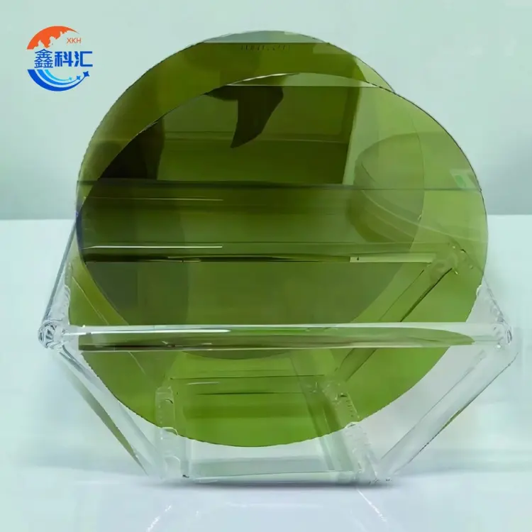
SiC wafers increased from 4-inch to 6-inch, and now 8-inch wafer production is expanding rapidly around the world.
Device diversification
SiC is no longer limited to discrete components. It is now used in:
- MOSFETs
- Schottky diodes
- JFETs
- Power modules for electric vehicles
- Integrated power systems and gate drivers
Supply chain maturation
A complete ecosystem has emerged, covering raw materials, crystal growth, epitaxy, chip design, and power module packaging.
Wider application scenarios
SiC now plays vital roles in:
- EV traction inverters
- Fast-charging stations
- Photovoltaic inverters
- ระบบกักเก็บพลังงาน
- Aerospace electronics
- Industrial motor drives
- 5G base stations
SiC has become the material enabling higher efficiency, smaller systems, and lower energy loss across nearly all high-power applications.
7. The Future: Toward a New Era of High-Efficiency Power Electronics
Silicon Carbide will continue shaping the technological landscape in several key directions.
Larger wafers and lower costs
8-inch wafers are becoming the new industry standard, dramatically increasing yield and reducing production cost.
Improved crystal quality
Defect reduction technologies will enable higher reliability for automotive-grade and aerospace-grade devices.
Advanced packaging
Full-SiC power modules and optimized thermal designs will push performance beyond what silicon-based systems can achieve.
Integration with other materials
SiC will coexist with Silicon and GaN, each occupying its own performance window, forming a balanced semiconductor ecosystem.
Extreme-environment electronics
SiC’s ability to operate at high temperatures, high radiation, and high voltage makes it ideal for next-generation aerospace, deep-space missions, and harsh industrial environments.
สรุป
The evolution of Silicon Carbide reflects the broader history of materials science. What began as an accidental by-product has become a key enabler of global electrification and energy transformation. From grinding wheels to electric vehicles, from furnace linings to space-grade electronics, SiC continues to push the boundaries of what materials can achieve.
As the world moves toward cleaner energy and more efficient power systems, Silicon Carbide will remain at the center of innovation—driving progress in industries that define the future of technology.