
Silicon carbide (SiC) has become one of the most important semiconductor materials for high-power, high-voltage and high-frequency applications. As electric vehicles, renewable energy systems, AI power supplies and industrial automation continue to grow, the demand for larger SiC substrates is increasing rapidly. Compared with traditional 6-inch wafers, 8-inch (200 mm) SiC wafers provide more usable die area, improved manufacturing efficiency and lower cost per chip, making them the preferred platform for next-generation semiconductor production.
However, selecting an 8-inch SiC wafer involves much more than simply choosing the wafer diameter. Buyers must carefully evaluate thickness, crystal orientation, electrical properties, surface quality, defect density and mechanical tolerances to ensure compatibility with epitaxy and device fabrication processes.
This guide explains the key specifications every semiconductor buyer should understand before requesting a quotation for 8-inch SiC wafers.
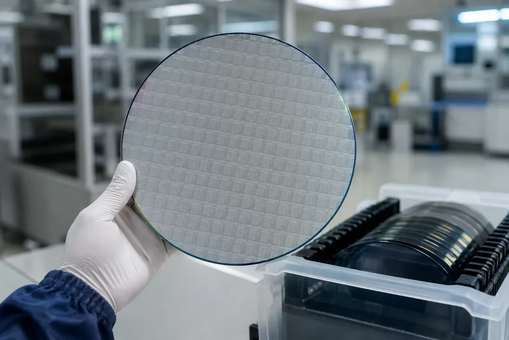
Why Are 8-Inch SiC Wafers Becoming the Industry Standard?
For many years, 4-inch and 6-inch SiC wafers dominated the power semiconductor industry. Today, leading manufacturers are transitioning toward 8-inch substrates to increase production capacity and reduce manufacturing costs.
The advantages of 8-inch SiC wafers include:
- Higher chip output per wafer
- Lower cost per device
- Improved equipment productivity
- Better manufacturing efficiency
- Reduced edge loss
- Greater competitiveness for mass production
As automotive manufacturers expand electric vehicle production and data centers require more efficient power conversion systems, the adoption of 200 mm SiC substrates is expected to accelerate significantly.
Standard Dimensions of an 8-Inch SiC Wafer
Although individual manufacturers may define slightly different specifications, the following parameters are commonly accepted within the semiconductor industry.
| Şartname | Tipik Değer |
|---|---|
| Wafer Diameter | 200 mm (8 inch) |
| Diameter Tolerance | ±0.20 mm |
| Kalınlık | 500–725 μm |
| Kristal Yapı | 4H-SiC |
| Yüzey İşlemi | SSP or DSP |
| Oryantasyon | On-axis or 4° Off-axis |
| Primary Flat / Notch | According to SEMI Standard |
| Edge Profile | Rounded Edge |
Different applications may require customized thicknesses or orientation angles depending on the epitaxial growth process.
Thickness Specifications
Wafer thickness directly influences mechanical stability, polishing performance and compatibility with semiconductor equipment.
Typical thickness options include:
| Kalınlık | Tipik Uygulama |
| 500 μm | Thin wafer processing |
| 600 μm | Standard production |
| 650 μm | Power devices |
| 725 μm | High rigidity applications |
Thickness tolerance is generally controlled within a few micrometers to maintain excellent flatness during lithography and epitaxy.
Electrical Specifications
Electrical properties are determined by the wafer type and intended application.
N-Type Conductive SiC Wafer
Typical parameters include:
- Polytype: 4H-SiC
- Dopant: Nitrogen (N)
- Resistivity:
- 0.015–0.028 Ω·cm
- 0.018–0.025 Ω·cm
- Carrier Concentration:
- Approximately 1×10¹⁸ cm⁻³
These wafers are widely used for:
- SiC MOSFET'ler
- Schottky Barrier Diodes
- Power Modules
- Fast Chargers
- Solar Inverters
Semi-Insulating SiC Wafer
Tipik teknik özellikler şunlardır:
- Resistivity:1×10⁵ Ω·cm
veya
1×10⁸ Ω·cm
depending on the application.
Semi-insulating substrates are commonly used for:
- RF Devices
- GaN-on-SiC Epitaxy
- Microwave Devices
- Radar Systems
- 5G Base Stations
Surface Quality Specifications
Surface quality has a direct impact on epitaxial growth and device yield.
Important specifications include:
| Parametre | Tipik Gereksinim |
| Yüzey Pürüzlülüğü (Ra) | ≤0.2 nm |
| TTV | ≤10 μm |
| Yay | ≤20 μm |
| Warp | ≤30 μm |
| Edge Chips | Hiçbiri |
| Scratches | According to customer specification |
A high-quality polished surface minimizes crystal defects during epitaxial deposition and improves device reliability.
Defect Limits Buyers Should Pay Attention To
Crystal defects significantly affect semiconductor yield and long-term device reliability.
The most important defects include:
Micropipes (MP)
Micropipes are hollow-core crystal defects that can cause catastrophic device failure. Modern production-grade wafers typically require extremely low micropipe densities.
Bazal Düzlem Dislokasyonları (BPD)
BPDs may expand during bipolar device operation, reducing device lifetime and reliability.
Vida Çıkıkları (TSD)
TSDs influence leakage current and overall crystal quality.
Kenar Dislokasyonlarının İpliklenmesi (TED)
Although less harmful than micropipes, excessive TED density can still affect epitaxial uniformity.
Typical defect specifications are summarized below.
| Kusur Türü | Tipik Gereksinim |
| Mikro Boru Yoğunluğu | Extremely Low or Zero |
| BPD Density | According to Grade |
| TSD Density | Controlled |
| TED Density | Controlled |
| Surface Defects | Customer Specification |
Different grades such as Production Grade, Research Grade and Dummy Grade have different defect limits.
SSP vs DSP Surface Finish
Surface finish selection depends on downstream manufacturing requirements.
SSP (Single Side Polished)
Özellikleri:
- One polished surface
- Lower cost
- Suitable for epitaxy
Uygulamalar:
- Device manufacturing
- Epitaxial growth
DSP (Double Side Polished)
Özellikleri:
- Both surfaces polished
- Better flatness
- Higher alignment accuracy
Uygulamalar:
- Wafer bonding
- MEMS
- Optical devices
- Advanced packaging
Typical Applications of 8-Inch SiC Wafers
As production capacity expands, 8-inch SiC wafers are increasingly used in:
- Electric Vehicle Power Modules
- High-Voltage MOSFETs
- Schottky Barrier Diodes
- AI Server Power Supplies
- Renewable Energy Systems
- Industrial Motor Drives
- Railway Traction Systems
- Havacılık ve Uzay Elektroniği
- RF Devices
- High-Power Converters
The larger wafer size enables manufacturers to increase chip output while reducing overall production costs.
RFQ Checklist for 8-Inch SiC Wafers
To receive an accurate quotation, buyers should provide as much technical information as possible.
A complete RFQ typically includes:
- Gofret çapı
- Kalınlık
- Polytype (4H-SiC)
- Conductive or Semi-Insulating
- Dirençlilik
- Crystal orientation
- Off-axis angle
- Surface finish (SSP/DSP)
- TTV requirement
- Bow requirement
- Warp requirement
- Yüzey pürüzlülüğü
- Defect limits
- Wafer grade
- Quantity
- Packaging requirements
- Delivery schedule
Providing complete specifications helps suppliers recommend the most suitable products and reduces unnecessary communication.
How to Choose the Right Supplier
When evaluating an SiC wafer supplier, buyers should consider more than just pricing.
Key evaluation factors include:
- Manufacturing capability
- Crystal quality consistency
- Defect inspection reports
- Traceability
- Quality management system
- Packaging standards
- Technical support
- Customization capability
- Stable long-term supply
A supplier capable of providing detailed inspection reports, customized specifications and responsive engineering support is often more valuable than one offering only the lowest price.
Frequently Asked Questions
What is the standard diameter of an 8-inch SiC wafer?
The standard diameter is 200 mm, commonly referred to as an 8-inch wafer.
What thickness is commonly available?
Standard thicknesses range from 500 μm to 725 μm, with customized options available for specific applications.
What is the difference between conductive and semi-insulating SiC wafers?
Conductive wafers are primarily used for power semiconductor devices, while semi-insulating wafers are widely used in RF and microwave applications.
Which surface finish should I choose?
SSP is suitable for most epitaxial processes, while DSP is preferred for wafer bonding, MEMS and applications requiring both surfaces to be polished.
Which specifications are most important when purchasing 8-inch SiC wafers?
The most critical specifications include diameter, thickness, resistivity, crystal orientation, surface finish, TTV, bow, warp, defect limits and wafer grade.
Sonuç
The transition from 6-inch to 8-inch SiC wafers represents a major milestone in semiconductor manufacturing. Larger substrates enable higher productivity, lower production costs and greater scalability for power electronics and advanced semiconductor devices.
Before placing an order, buyers should carefully review key specifications such as wafer dimensions, electrical properties, crystal orientation, surface quality and defect limits. Providing complete RFQ information not only accelerates supplier evaluation but also helps ensure that the selected wafer meets the performance and reliability requirements of the final application.
Whether your project involves power devices, RF components or advanced packaging, selecting the appropriate 8-inch SiC wafer specifications is essential for achieving consistent manufacturing quality and long-term device performance.