
In the evolving landscape of advanced materials, few substances demonstrate the breadth of capabilities seen in silisyum karbür (SiC). Often categorized as a third-generation semiconductor, SiC is widely recognized for its role in high-efficiency power electronics. However, limiting SiC to this single application underestimates its full potential.
What makes SiC exceptional is its multi-domain performance across optical, thermal, chemical, and electrical properties—a rare combination that enables it to solve engineering bottlenecks in some of the most demanding industries today, including augmented reality (AR), space exploration, and quantum computing.
This article explores how the intrinsic atomic structure of SiC translates into real-world advantages and how these properties directly address critical technological pain points.
The Structural Origin of SiC’s “All-in-One” Properties
At the core of SiC’s performance lies its sp³ hybridized covalent bonding structure. Both silicon (Si) and carbon (C) belong to Group IV of the periodic table, each contributing four valence electrons. When combined, they form a three-dimensional tetrahedral network, where each atom is strongly bonded to four neighbors.
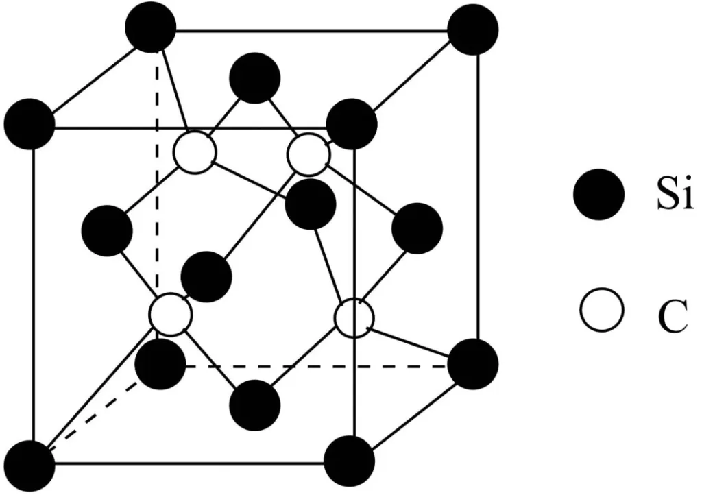
This structure results in:
- High bond energy (~4.6 eV) → exceptional mechanical strength and thermal stability
- Short bond length → dense and rigid lattice
- Wide bandgap (~3.26 eV for 4H-SiC) → excellent electrical insulation and high breakdown voltage
- Strong lattice stability → resistance to chemical and radiation damage
Unlike materials such as SiO₂ or AlN, subtle differences in atomic size and electronegativity in SiC lead to a unique balance of properties across multiple physical domains.
Electrical and Thermal Superiority: Powering the Next Generation
Before exploring emerging applications, it’s important to understand why SiC dominates in power electronics, which forms the foundation for its expansion into other fields.
Key Advantages:
- Breakdown electric field: ~10× higher than silicon
- On-resistance: up to 90% lower
- Çalışma sıcaklığı: stable above 175°C
- Termal iletkenlik: ~3× higher than silicon
These characteristics enable:
- Smaller device geometries
- Daha yüksek anahtarlama frekansları
- Reduced cooling requirements
Applications such as EV inverters, onboard chargers, and 800V fast-charging platforms have already proven these advantages in real-world systems.
Silicon Carbide in AR Displays: Breaking Optical Bottlenecks
The Problem:
Current AR devices struggle with:
- Limited field of view (FoV)
- Image distortion and “rainbow artifacts”
- Bulky optical modules
The SiC Solution:
Silicon carbide introduces a major breakthrough in optical waveguide technology:
- High refractive index (~2.6) vs. traditional glass (~1.8–1.9)
- Enables FoV > 80° with fewer optical layers
- Reduces chromatic dispersion and stray light
Real Impact:
- Slimmer AR glasses design
- More immersive visual experience
- Improved image clarity
As companies like Meta and Goertek continue developing SiC-based waveguides, the material is becoming a key enabler for next-generation wearable displays.
Space Exploration: Extreme Reliability in Harsh Environments
The Problem:
Space systems must operate under:
- Extreme temperature fluctuations
- High radiation exposure
- Severe weight constraints
The SiC Solution:
1. High-Efficiency Power Systems
SiC-based electronics:
- Increase power density by up to 5×
- Reduce system size and weight
- Improve mission efficiency and payload capacity
2. Structural and Optical Stability
SiC is ideal for:
- Telescope mirrors
- Optical sensors
Thanks to:
- Low thermal expansion
- High stiffness-to-weight ratio
Real Impact:
- Reduced launch costs
- Enhanced deep-space mission reliability
- Improved imaging accuracy
SiC is already being considered for future lunar and deep-space exploration systems.
Quantum Technologies: Enabling Scalable Quantum Systems
The Problem:
Many quantum systems require:
- Ultra-low temperatures
- Complex and expensive infrastructure
- Limited scalability
The SiC Solution:
Silicon carbide supports defect-based quantum systems, particularly color centers such as:
- Silicon vacancies
- Divacancies
These defects act as quantum bits (qubits).
Unique Advantages:
1. Room-Temperature Operation
Unlike superconducting qubits, SiC systems can function in near-ambient conditions.
2. Long Coherence Time
- Nuclear spins (e.g., ²⁹Si, ¹³C) act as quantum memory
- Enable stable and long-lived information storage
3. Telecom-Compatible Photon Emission
- Emission near 1550 nm wavelength
- Compatible with existing fiber optic infrastructure
Real Impact:
- Enables quantum communication networks
- Reduces system complexity and cost
- Accelerates commercialization of quantum technologies
Institutions like Fraunhofer Society are actively researching SiC-based quantum devices for scalable architectures.
Beyond Electronics: SiC in Fusion Energy and Extreme Materials
Beyond semiconductors, SiC is also emerging as a critical material in nuclear fusion systems:
- Used in plasma-facing components
- Withstands extreme radiation and thermal loads
- Maintains structural integrity under neutron bombardment
Companies like Kyocera are developing advanced SiC composites for fusion reactors, while energy innovators such as Helion Energy are testing its long-term reliability in real-world conditions.
Conclusion: A Platform Material for Future Technologies
Silicon carbide is no longer just a “better silicon.” Its multi-functional capabilities across light, heat, chemistry, and electricity position it as a foundational material for next-generation technologies.
From enabling immersive AR experiences to supporting deep-space missions and advancing quantum networks, SiC is solving challenges that traditional materials simply cannot address.
As industries continue to demand higher efficiency, smaller form factors, and greater reliability, silicon carbide stands out as a platform material shaping the future of engineering and innovation.