

Mô tả
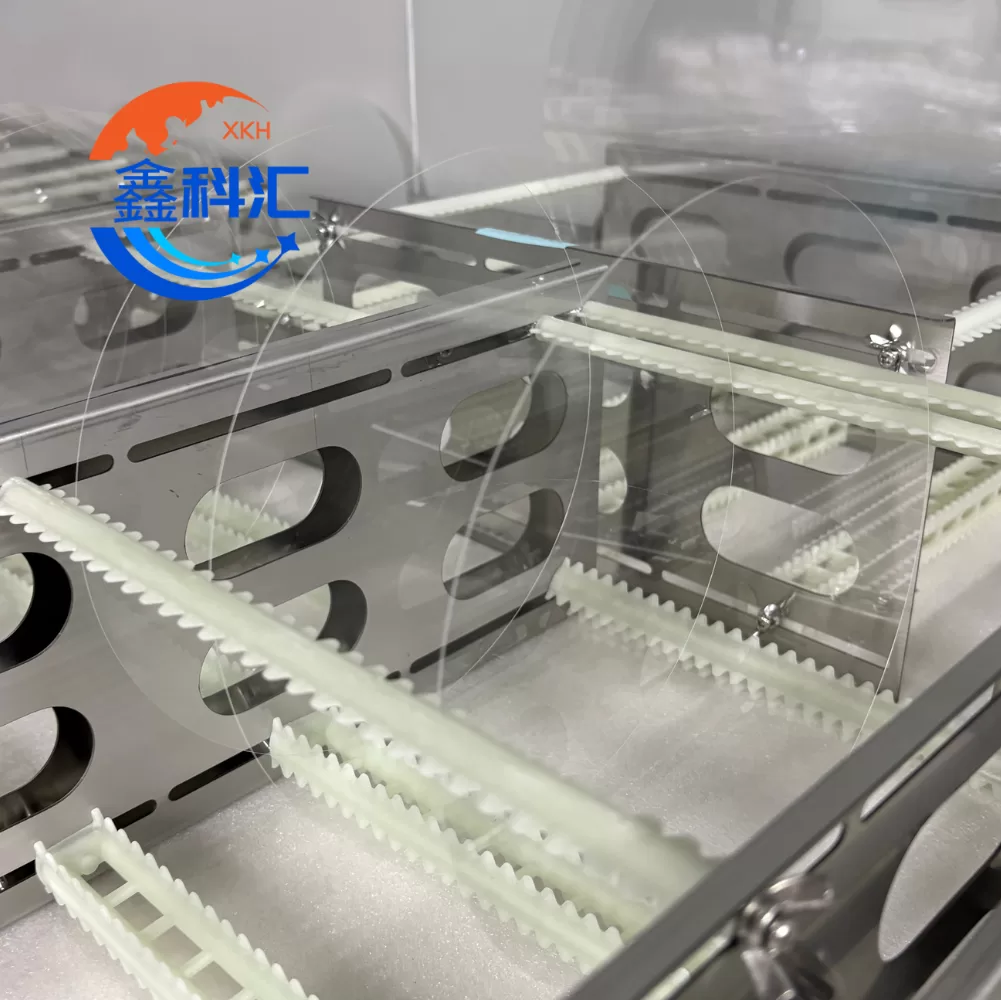
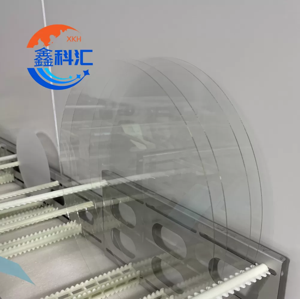
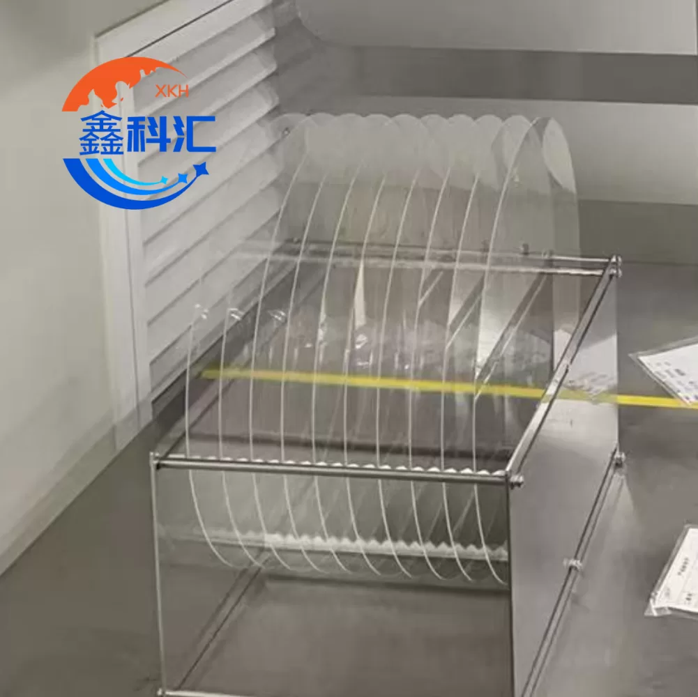
 The 12 inch glass substrate is a high precision engineered material widely used in advanced semiconductor packaging, MEMS devices, photonic integration, and optical systems. With the rapid development of large scale integration technologies and wafer level processes, glass substrates have become a key enabling material for next generation electronic and optical applications.
Compared with traditional silicon substrates, glass substrates offer excellent electrical insulation, low dielectric loss, high optical transparency, and superior dimensional stability. These characteristics make them particularly suitable for wafer level packaging, fan out wafer level packaging, and optical interconnection systems.
Our 12 inch glass substrates are available in multiple material systems including borosilicate glass, quartz, fused silica, and alkaline free glass. Each material is selected based on thermal, optical, and mechanical performance requirements.
Material Options
Borosilicate Glass Substrate
Borosilicate glass provides excellent thermal stability and silicon compatibility.
- Thermal expansion closely matched to silicon
- Suitable for anodic bonding processes
- High chemical resistance
- Stable under thermal cycling
- Ideal for MEMS and packaging structures
Quartz Glass Substrate
Quartz substrates are widely used in optical and high frequency applications.
- High UV to IR optical transmission
- Extremely low impurity content
- Surface roughness down to Ra ≤ 0.5 nm
- Khả năng chịu sốc nhiệt tuyệt vời
- Suitable for photonics and optical MEMS
Fused Silica Substrate
Fused silica is a high purity synthetic material designed for extreme environments.
- Ultra low thermal expansion
- High chemical purity
- Strong resistance to high temperature processing
- Optical transmission above 90 percent in wide spectrum
- Ideal for lithography and precision optics
Alkaline Free Glass Substrate
Designed for advanced electronics requiring ultra low contamination.
- Free from heavy metals and halides
- Low fluorescence background
- High dielectric stability
- Excellent chemical durability
- Compatible with semiconductor integration
Key Technical Specifications
Dimensions
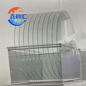
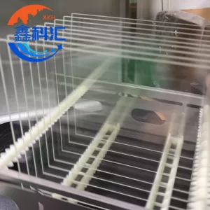
- Size 300 mm 12 inch standard
- Thickness range 500 microns to 2000 microns
- Thickness tolerance plus minus 5 to 20 microns
- Total thickness variation below 10 to 15 microns
- Custom edge profiles available
Chất lượng bề mặt
- Surface roughness Ra below 1.0 nm standard
- Ultra polished version down to Ra 0.5 nm
- Flatness up to lambda over 10 optional
- Single side or double side polished available
- Cleanroom grade processing
Material Performance Reference
| Vật liệu | Sự giãn nở nhiệt | Optical Transmission | Tính năng |
|---|---|---|---|
| Borosilicate | Thấp | Trung bình | Silicon bonding compatibility |
| Thạch anh | Rất thấp | Cao | Optical grade stability |
| Thạch anh hợp nhất | Ultra low | Rất cao | Độ tinh khiết cao |
| Alkaline Free | Trung bình | Varies | Low contamination |
 Ứng dụng
 Ứng dụng
12 inch glass substrates are widely used in:
- Wafer level packaging
- Fan out wafer level packaging
- MEMS sensors and actuators
- Photonic integrated circuits
- Optical communication systems
- Automotive sensing systems
- Display technologies OLED and MicroLED
- Biochips and lab on chip devices
- Các linh kiện tần số vô tuyến và vi sóng
- Precision optical systems
Ưu điểm
- Full compatibility with 300 mm manufacturing systems
- Excellent dimensional stability
- Ultra smooth surface below 1 nm roughness
- High optical and electrical performance
- Strong chemical and thermal resistance
- Flexible material selection
- Scalable from prototype to mass production
FAQ (Frequently Asked Questions)
Q1: What is a 12 inch glass substrate used for in semiconductor applications?
A 12 inch glass substrate is primarily used as a high precision platform in advanced semiconductor packaging and integration processes. It is widely applied in wafer level packaging, fan out wafer level packaging, MEMS fabrication, photonic devices, and optical interconnection systems. Unlike silicon, glass substrates provide excellent electrical insulation and optical transparency, making them suitable for applications where signal integrity and optical performance are critical.
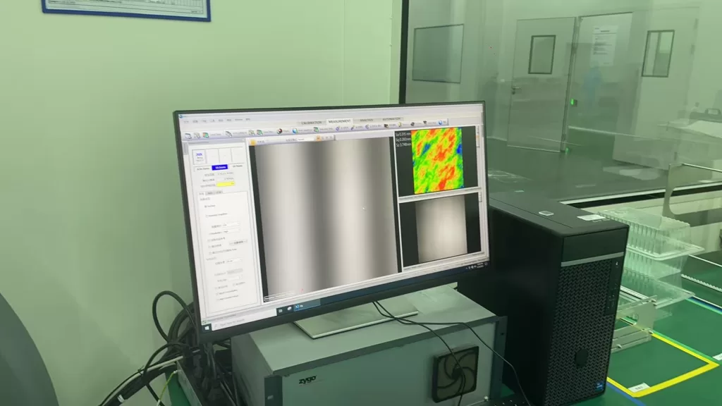
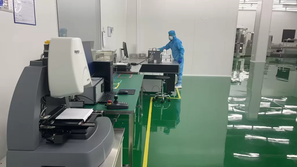
Q2: What surface quality and flatness can be achieved for 12 inch glass substrates?
Our 12 inch glass substrates are manufactured with high precision polishing and strict process control. Typical performance includes surface roughness (Ra) below 1.0 nm, with ultra polished grades reaching Ra 0.5 nm. Total thickness variation (TTV) can be controlled within 10 to 15 microns depending on material type and thickness. High end options can also achieve surface flatness up to lambda over 10, making them suitable for advanced lithography and bonding processes.
Q3: Can 12 inch glass substrates be customized for different process requirements?
Yes, full customization is available. We can adjust material type (borosilicate, quartz, fused silica, alkaline free glass), thickness, surface finish, edge profile, and flatness level according to customer requirements. Special processing such as single side polishing, double side polishing, laser marking, and alignment features can also be provided. This makes the substrates suitable for both R and D development and high volume manufacturing environments.
Đánh giá
Chưa có đánh giá nào.