
Mô tả
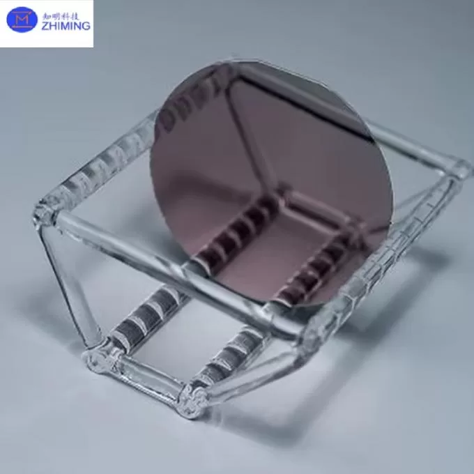
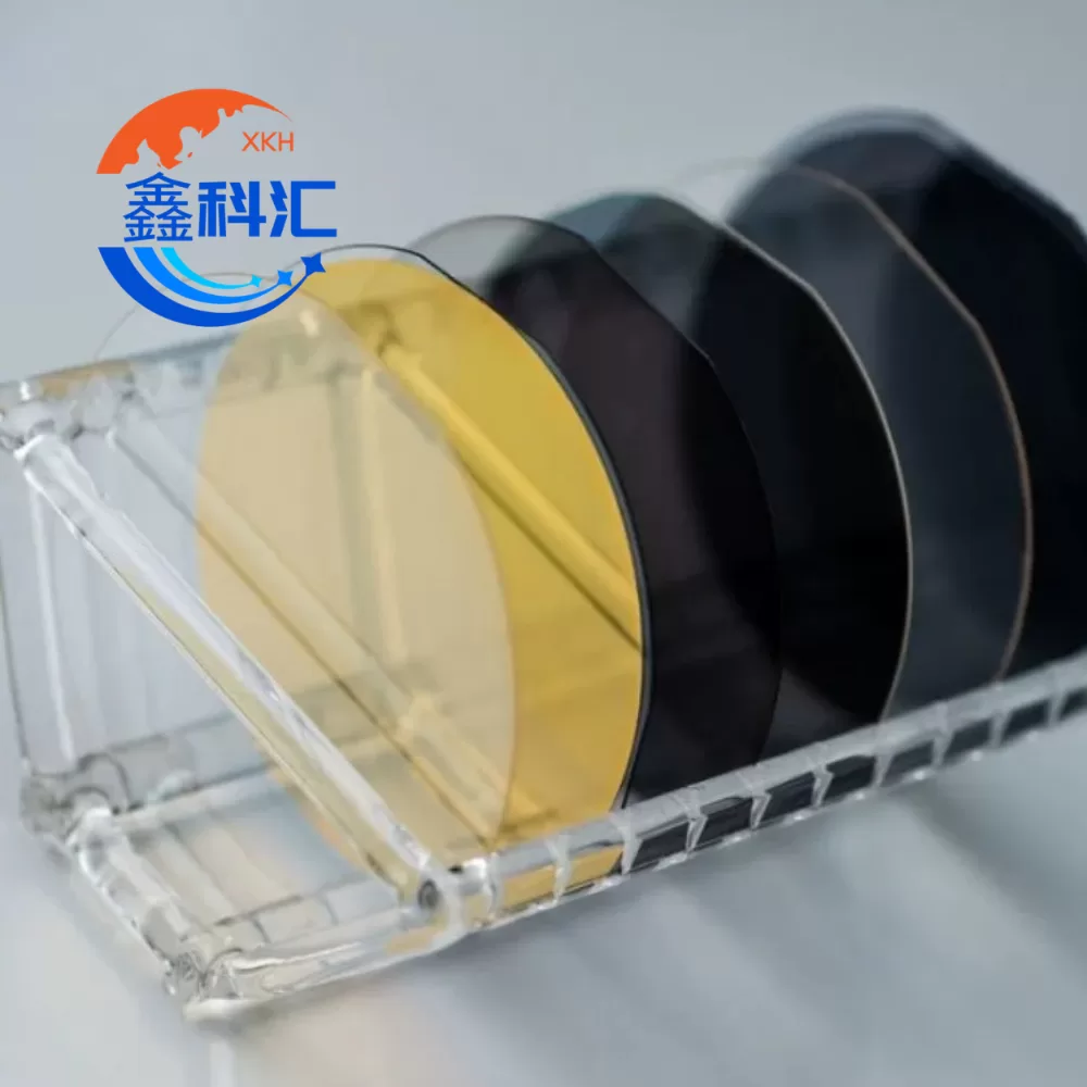
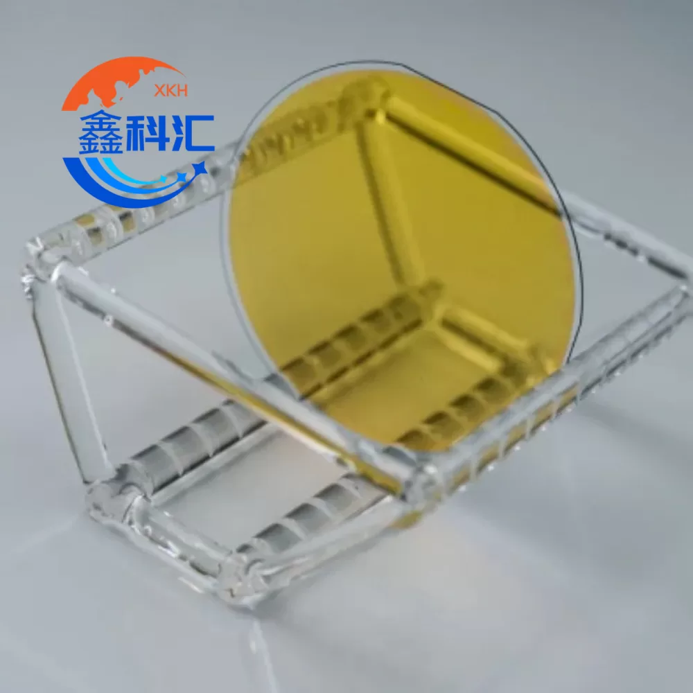
Thin-Film Lithium Niobate on Insulator (LNOI) is a wafer-scale photonic material platform based on a single-crystal lithium niobate thin film bonded to an insulating oxide layer and silicon-based handle substrate.
The platform is designed for high-density integrated photonic circuits, enabling strong optical confinement, high electro-optic response, and low propagation loss.
It is widely used in high-speed optical communication, quantum photonics, and microwave photonic systems
.


Thin-Film Lithium Niobate (TFLN)
Thin-Film Lithium Niobate (TFLN) refers to a sub-micron crystalline LiNbO₃ layer engineered for guided-wave photonic devices.
Compared to bulk lithium niobate, the thin-film structure provides:
- Strong optical mode confinement
- Enhanced electro-optic interaction efficiency
- Reduced device footprint
- Compatibility with silicon-based photonic integration
TFLN is the functional core layer of the LNOI platform.
Wafer Stack Structure
| Layer | Vật liệu | Function |
|---|---|---|
| Device Layer | LiNbO₃ Thin Film (TFLN) | Electro-optic modulation and nonlinear optics |
| Insulator Layer | SiO₂ (Buried Oxide) | Optical isolation and vertical confinement |
| Handle Substrate | Si / Quartz / Sapphire | Mechanical support and process compatibility |
Platform Characteristics
- Optical propagation loss: < 0.05 dB/cm @ 1550 nm
- Thin-film thickness: 300 nm – 1000 nm
- Electro-optic coefficient: r₃₃ up to 90 pm/V
- Sub-micron waveguide compatibility
- CMOS-compatible photonic integration
- High thermal stability (~1140°C Curie temperature)
- Crystal cuts: X-cut / Y-cut / Z-cut
- Wafer formats: 3 inch / 4 inch / 6 inch / 8 inch
Wafer Specifications
Mechanical and Dimensional Properties
| Tham số | Thông số kỹ thuật |
|---|---|
| Wafer Diameter | 3″, 4″, 6″, 8″ |
| Total Thickness | 525 ± 25 μm |
| Bow | ±50 μm |
| Biến dạng | <50 μm |
| LTV | <1.5 μm (5×5 mm², 95%) |
Thin-Film Layer Properties
| Tham số | Thông số kỹ thuật |
|---|---|
| Vật liệu | Single-crystal LiNbO₃ |
| Độ dày | 300 nm – 1000 nm |
| Orientation Tolerance | ±0.5° |
| Độ nhám bề mặt | Ra < 1 nm |
| Mật độ khuyết tật | No voids >1 mm |
Buried Oxide Layer
| Tham số | Thông số kỹ thuật |
|---|---|
| Vật liệu | Silic dioxit |
| Thickness Range | 100 nm – 2 μm |
| Uniformity | ±5% |
Fabrication Flow
LNOI wafers are manufactured using semiconductor-compatible processing technologies:
- Ion implantation for controlled layer separation in bulk LiNbO₃
- Wafer bonding onto oxide-coated handle substrates
- High-temperature annealing for crystal recovery
- Chemical Mechanical Polishing (CMP) for surface planarization
- Full-wafer metrology and optical characterization
Application Domains
Integrated photonic circuits for high-speed optical communication systems (100G–800G)
Quantum photonic platforms for entangled photon generation and quantum information processing
Microwave photonic systems for RF signal processing and millimeter-wave photonics
Nonlinear optical systems including frequency conversion and optical frequency comb generation
Integrated optical sensing systems for biochemical and environmental detection
Performance Comparison
| Tài sản | Bulk LiNbO₃ | LNOI Platform |
|---|---|---|
| Optical Loss | Higher | <0.05 dB/cm |
| Integration Density | Thấp | Cao |
| Device Footprint | Large | Compact (sub-micron) |
| CMOS Compatibility | Not compatible | Compatible |
| Electro-optic Efficiency | Trung bình | High (Vπ ~ 1V) |
Engineering Flexibility
Crystal orientation: X-cut, Y-cut, Z-cut configurations available
Thin-film thickness engineering from 300 nm to 1 μm
Buried oxide thickness tuning for mode confinement optimization
Substrate selection including silicon, quartz, and sapphire
Optional MgO doping for enhanced optical damage resistance
Metrology and Quality Control
Optical loss characterization at telecom wavelengths
Surface roughness measurement using AFM
Bonding interface inspection via infrared imaging
Thickness uniformity mapping across full wafer
Wafer flatness and stress distribution analysis
Engineering Support
ZMSH provides integrated support across the LNOI platform lifecycle, including material design, wafer bonding process development, photonic device fabrication assistance, nanofabrication processes (EBL, IBE), and optical performance validation.
Production capability includes stable 6-inch wafer manufacturing and scalable development toward 8-inch LNOI platforms for advanced photonic integration.
Frequently Asked Questions
What is the function of LNOI wafers?
LNOI wafers serve as integrated photonic platforms for optical communication, quantum photonics, nonlinear optics, and sensing applications.
What is the thickness of thin-film lithium niobate?
Typical film thickness ranges from 300 nm to 1000 nm depending on device requirements.
What advantages does LNOI offer over bulk lithium niobate?
LNOI enables lower optical loss, higher integration density, and compatibility with silicon photonic systems.
Is LNOI compatible with silicon photonics platforms?
Yes, LNOI is fully compatible with silicon and silicon nitride photonic integration.
Đánh giá
Chưa có đánh giá nào.