
Silicon Carbide (SiC), as a third-generation wide-bandgap semiconductor material, has gained significant importance in power electronics, including electric vehicles, photovoltaic inverters, high-voltage power supplies, and industrial energy systems.
Thanks to its wide bandgap, high breakdown electric field, and excellent thermal conductivity, SiC enables devices with higher efficiency, higher switching speed, and better high-temperature stability compared with traditional silicon.
However, SiC wafer manufacturing is extremely challenging. Due to the high growth temperature and complex crystal growth dynamics, various types of crystal defects are inevitably introduced during production. These defects can significantly affect wafer yield, device performance, and long-term reliability.
Understanding these defects is essential for both substrate manufacturers and device engineers.
1. Origin of SiC Wafer Defects
Most commercial SiC wafers are grown using the Physical Vapor Transport (PVT) method, which operates at extremely high temperatures (above 2000°C).
During crystal growth and wafer processing, defects may originate from:
- Instability in crystal growth conditions
- Thermal stress during cooling
- Impurities in source materials
- Lattice mismatch and dislocations
- Mechanical damage during slicing and polishing
Because SiC has strong covalent bonding and a very high melting point, defect elimination is significantly more difficult than in silicon.
2. Common Types of SiC Wafer Defects
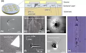
2.1 Micropipes
Micropipes are hollow-core screw dislocations that extend through the crystal.
特性:
- Hollow tubular structure
- Threading along the crystal growth direction
- Easily propagated during growth
Impact on devices:
- Severe leakage current
- Catastrophic device failure
- 擊穿電壓降低
Micropipes were once a major limitation in early SiC technology, though their density has been greatly reduced in modern wafers.
2.2 Threading Screw Dislocations (TSD)
TSDs are line defects that propagate along the crystal growth axis.
Impact on devices:
- 增加漏電電流
- Reduced reliability in high-voltage devices
- Local electric field concentration
They are particularly critical in high-power MOSFET applications.
2.3 Threading Edge Dislocations (TED)
TEDs are one of the most common defect types in SiC wafers.
Impact on devices:
- Moderate effect on leakage current
- Degradation of carrier mobility
- Reduced channel stability in MOSFETs
Although less severe than micropipes, their high density makes them important.
2.4 Basal Plane Dislocations (BPD)
BPDs lie in the basal plane of the crystal structure.
Impact on devices:
- Bipolar degradation (especially in diodes and IGBTs)
- Increased forward voltage drift over time
- Reduced long-term reliability
BPD conversion into stacking faults during operation is a major reliability concern in power devices.
2.5 Stacking Faults
Stacking faults are planar defects caused by disruptions in crystal layer stacking.
Impact on devices:
- Increased on-resistance
- Reduced current capability
- Long-term performance degradation
They are often linked with BPD propagation under electrical stress.
2.6 Polytype Inclusions
SiC has multiple polytypes (e.g., 4H-SiC, 6H-SiC). Improper growth may cause mixed polytype regions.
Impact on devices:
- Local variation in bandgap
- Unstable electrical behavior
- Reduced device consistency
3. Impact of Defects on Device Performance
SiC device performance is highly sensitive to crystal quality. Even low-density defects can significantly affect electrical behavior.
3.1 Breakdown Voltage Reduction
Defects such as micropipes and TSDs create local electric field concentration, leading to premature breakdown.
3.2 Increased Leakage Current
Dislocation cores act as leakage paths, increasing off-state current in power devices.
3.3 Reliability Degradation
Defects such as BPDs and stacking faults can evolve during device operation, causing:
- 正向電壓漂移
- Increased on-resistance over time
- Device aging under electrical stress
3.4 Reduced Yield in Power Device Manufacturing
Even a small defect density can result in:
- Lower wafer utilization
- Reduced die yield
- 較高的生產成本
4. Defect Control and Reduction Strategies
Modern SiC manufacturing has significantly improved defect control through:
4.1 Improved Crystal Growth Techniques
- Optimized PVT growth conditions
- Controlled temperature gradients
- High-purity raw materials
4.2 Defect Conversion Techniques
- Converting BPDs into harmless dislocations
- Reducing propagation of threading defects
4.3 Advanced Wafer Characterization
- X-ray topography
- Photoluminescence mapping
- Infrared microscopy
- KOH etching inspection
4.4 Epitaxial Layer Engineering
Epitaxial growth can reduce the impact of substrate defects by:
- Filtering dislocations
- Improving surface quality
- Enhancing device uniformity
5.產業趨勢
As SiC moves toward:
- 8-inch wafer production
- Automotive-grade reliability standards
- Higher voltage (1200V–3300V) applications
Defect density requirements are becoming increasingly strict.
Modern industry targets include:
- Micropipes: near zero
- BPD density: significantly reduced
- Improved wafer uniformity
This trend is critical for large-scale EV adoption and high-efficiency power systems.
總結
SiC wafer defects remain one of the most critical challenges in wide-bandgap semiconductor manufacturing. Although significant progress has been made in reducing micropipes and dislocation densities, defects such as BPDs, TEDs, and stacking faults still play a key role in determining device performance and reliability.
A deep understanding of these defects is essential for both material engineers and device designers. By improving crystal growth techniques and optimizing epitaxial processes, the industry continues to push SiC technology toward higher efficiency, greater reliability, and broader industrial adoption.