gan on sapphire wafer: sapphire with gallium nitride substrates
particularly in high-voltage applications, such as those requiring vertical gan devices with ratings more than 600 v, vertical gan power devices can potentially transform the power device market. gan devices have a lower on-resistance at a given breakdown voltage compared to both classic silicon-based power devices and upcoming pure silicon carbide power devices, depending on the material’s physical features. in the low-voltage market, horizontal gan power devices, also known as gan-on-silicon high mobility transistors (hemts), compete with silicon devices, and gan is superior, further demonstrating the superiority of gan materials.
Gallium Nitride on Sapphire, often abbreviated as GaN on Sapphire, represents a groundbreaking advancement in semiconductor technology. This innovative combination harnesses the unique properties of gallium nitride (GaN) while utilizing sapphire as the substrate material. In this comprehensive product introduction, we will explore the key features, advantages, applications, and the transformative impact of GaN on Sapphire in the semiconductor industry.
Key Features:
Material Synergy:
GaN on Sapphire leverages the synergy between gallium nitride and sapphire. Gallium nitride provides excellent electrical properties, while sapphire serves as a robust and thermally efficient substrate, creating a powerful combination for semiconductor applications.
Wide Bandgap Semiconductor:
GaN is known for its wide bandgap, a crucial characteristic that allows for high-temperature operation and efficient power handling. This property makes GaN on Sapphire well-suited for applications requiring high-power and high-frequency operation.
Thermal Stability:
Sapphire’s exceptional thermal stability complements GaN’s high-temperature capabilities. This combination ensures reliable performance even under extreme operating conditions, making GaN on Sapphire suitable for demanding applications.
High Electron Mobility:
GaN exhibits high electron mobility, enabling fast electron movement within the semiconductor material. This results in efficient and high-speed electronic devices, making GaN on Sapphire ideal for applications demanding rapid signal processing.
Low Dislocation Density:
The use of sapphire as a substrate contributes to low dislocation density in GaN on Sapphire structures. This feature enhances the material quality and reliability, leading to improved device performance and longevity.
Advantages:
Power Efficiency:
GaN on Sapphire’s superior electrical properties translate to enhanced power efficiency. Devices built on this platform demonstrate reduced power losses, making them energy-efficient and environmentally friendly.
High-Frequency Operation:
The wide bandgap of GaN allows for high-frequency operation, making it suitable for applications in radio frequency (RF) devices, telecommunications, and high-frequency power electronics.
Miniaturization and Integration:
GaN on Sapphire enables the development of smaller and more compact devices due to its high electron mobility and efficient power handling. This feature facilitates the miniaturization and integration of semiconductor components.
Improved Reliability:
The low dislocation density in GaN on Sapphire contributes to improved device reliability. This is particularly crucial in applications where consistent and dependable performance is paramount.
Versatility Across Industries:
GaN on Sapphire finds applications across diverse industries, including telecommunications, automotive, aerospace, and power electronics. Its versatility makes it a preferred choice for next-generation semiconductor devices.
Applications:
RF Power Amplifiers:
GaN on Sapphire is widely used in the development of RF power amplifiers for wireless communication systems. Its high-frequency operation and power efficiency make it instrumental in enhancing signal strength in communication networks.
Power Electronics:
In power electronics applications, GaN on Sapphire is employed for the production of high-performance transistors and converters. Its efficiency and reliability contribute to the advancement of power management systems.
LEDs and Lighting:
GaN on Sapphire is a key technology in the manufacturing of high-brightness LEDs. Its wide bandgap is well-suited for emitting light in the visible spectrum, making it essential for energy-efficient lighting solutions.
Aerospace and Defense:
The robustness and reliability of GaN on Sapphire make it suitable for aerospace and defense applications. It is used in radar systems, electronic warfare, and high-frequency communication devices.
Automotive Electronics:
GaN on Sapphire is increasingly integrated into automotive electronics for power conversion and management. Its ability to operate at high temperatures and handle high power levels aligns with the demanding requirements of automotive applications.
Transformative Impact:
5G Technology:
GaN on Sapphire plays a pivotal role in the development of 5G technology. Its high-frequency capabilities contribute to the creation of efficient and high-performance RF devices essential for 5G communication networks.
Electric Vehicles:
The automotive industry benefits from GaN on Sapphire in the electrification of vehicles. Its use in power electronics enhances the efficiency and performance of electric vehicle systems.
Efficient Power Distribution:
GaN on Sapphire is transforming power distribution systems by enabling the development of compact and efficient power converters. This has implications for renewable energy systems and smart grid technologies.
Advancements in Lighting:
The use of GaN on Sapphire in LED technology has led to significant advancements in energy-efficient lighting solutions. It contributes to the development of brighter, longer-lasting, and environmentally friendly lighting options.
Future Trends:
Integration in Consumer Electronics:
GaN on Sapphire is expected to play a larger role in consumer electronics, leading to the development of smaller, more efficient devices in areas such as smartphones, laptops, and wearables.
Continued Expansion in 5G Infrastructure:
With the global rollout of 5G networks, the demand for GaN on Sapphire is expected to surge, driving further innovation in RF power amplifiers and high-frequency devices.
Emergence in Quantum Computing:
GaN on Sapphire’s unique properties may find applications in emerging technologies, including quantum computing, where its reliability and efficiency can contribute to the development of advanced computing systems.
Conclusion:
In conclusion, GaN on Sapphire stands at the forefront of semiconductor technology, offering a potent combination of gallium nitride’s electrical prowess and sapphire’s substrate advantages. Its impact spans diverse industries, from telecommunications to automotive and beyond. As the demand for high-frequency, efficient, and reliable semiconductor devices continues to rise, GaN on Sapphire is poised to play a pivotal role in shaping the future of electronic systems and technologies.
to compete in the high-voltage market with pure silicon carbide power devices, vertical gan power devices are being developed. several businesses have increased production of 6-inch and 8-inch sic in the first two years, and sic devices have earned some market share in the high-voltage application sector. on the other hand, vertical gan devices are not yet on the market, and only a select few manufacturers can produce gan wafers with a 4-inch diameter. for vertical gan devices to advance, it is essential to increase the availability of high-quality gan wafers. gallium nitride high voltage power devices may offer three benefits: the predicted on-resistance is much lower than the experimental one under a fixed breakdown voltage. that’s why the forward bias power loss is lower and the overall energy efficiency is better.
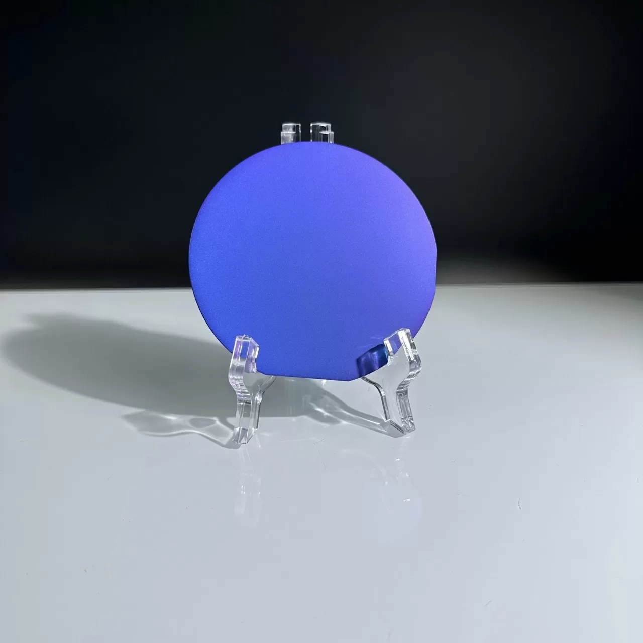
150mm 6inch GaN on Silicon/Sapphire/SiC Epi-layer wafer Gallium nitride epitaxial wafer
The 6-inch sapphire substrate wafer is a high-quality semiconductor material consisting of gallium nitride (GaN) layers grown on a sapphire substrate. The material has excellent electronic transport properties and is ideal for manufacturing high-power and high-frequency semiconductor devices.
150mm 6inch GaN on Silicon/Sapphire/SiC Epi-layer wafer Gallium nitride epitaxial wafer
The 6-inch sapphire substrate wafer is a high-quality semiconductor material consisting of layers of gallium nitride (GaN) grown on a sapphire substrate. The material has excellent electronic transport properties and is ideal for manufacturing high-power and high-frequency semiconductor devices.
Manufacturing method: The manufacturing process involves growing GaN layers on a sapphire substrate using advanced techniques such as metal-organic chemical vapor deposition (MOCVD) or molecular beam epitaxy (MBE). The deposition process is carried out under controlled conditions to ensure high crystal quality and uniform film.
6inch GaN-On-Sapphire applications: 6-inch sapphire substrate chips are widely used in microwave communications, radar systems, wireless technology and optoelectronics.
Some common applications include of GaN on Sapphire
Rf power amplifier
LED lighting industry
Wireless network communication equipment
Electronic devices in high temperature environment
Optoelectronic devices
Product specifications of GaN on Sapphire
Size: The substrate diameter is 6 inches (about 150 mm).
Surface quality: The surface has been finely polished to provide excellent mirror quality.
Thickness: The thickness of GaN layer can be customized according to specific requirements.
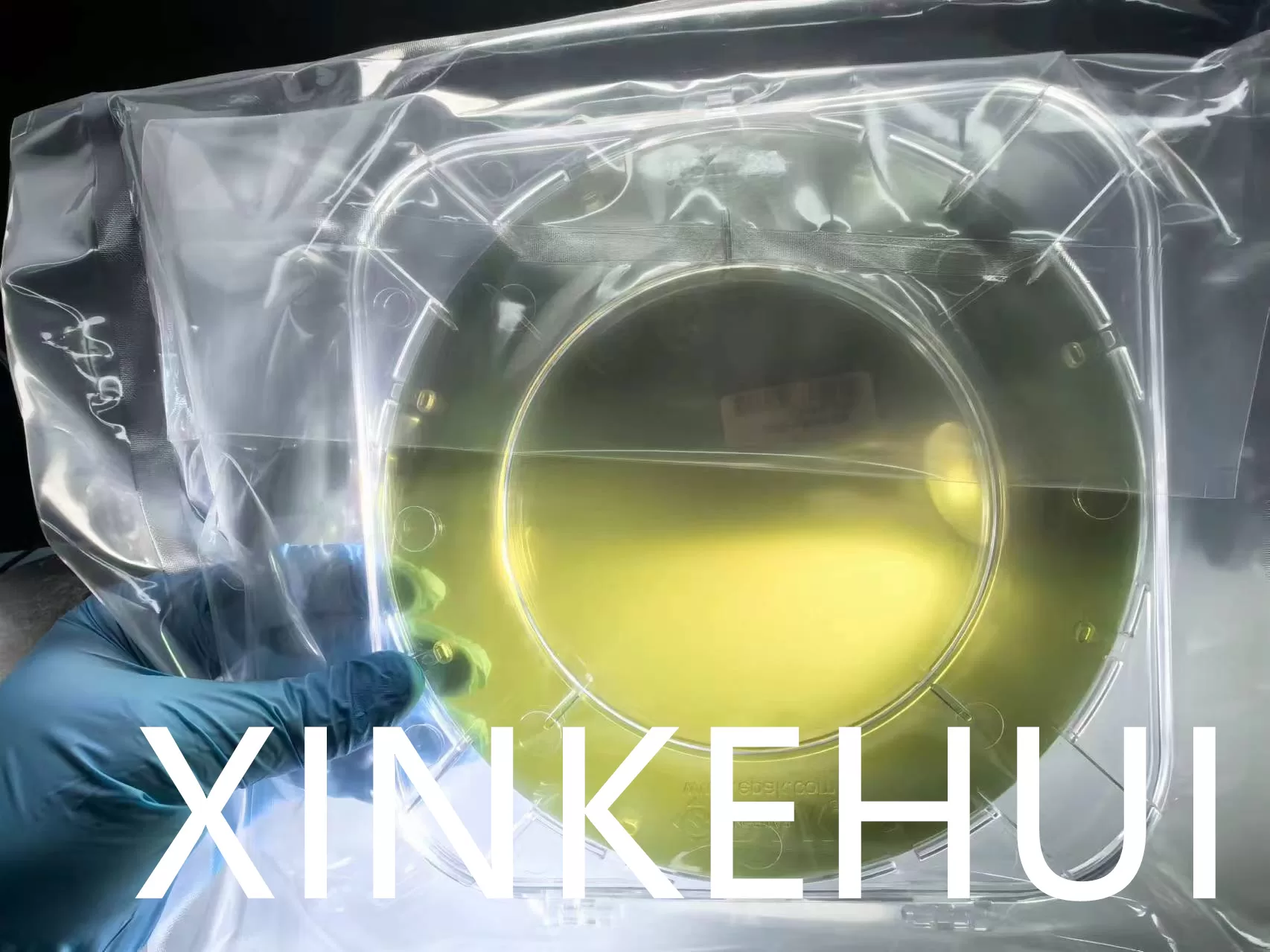
Packaging: The substrate is carefully packed with anti-static materials to prevent damage during transportation.
Positioning edges: The substrate has specific positioning edges that facilitate alignment and operation during device preparation
Other parameters: Specific parameters such as thinness, resistivity and doping concentration can be adjusted according to customer requirements.
With their superior material properties and diverse applications, 6-inch sapphire substrate wafers are a reliable choice for the development of high-performance semiconductor devices in various industries.
Substrate
6” 1mm <111> p-type Si
6” 1mm <111> p-type Si
Epi ThickAvg
~5um
~7um
Epi ThickUnif
<2%
<2%
Bow
+/-45um
+/-45um
Cracking
<5mm
<5mm
Vertical BV
>1000V
>1400V
HEMT Al%
25-35%
25-35%
HEMT ThickAvg
20-30nm
20-30nm
Insitu SiN Cap
5-60nm
5-60nm
2DEG conc.
~1013cm-2
~1013cm-2
Mobility
~2000cm2/Vs (<2%)
~2000cm2/Vs (<2%)
Rsh
<330ohm/sq (<2%)
<330ohm/sq (<2%)
GaN on Sapphire wafers
GaN on Sapphire wafers
GaN on sapphire Wafers
Why is GaN on Sapphire?
Compared to traditional silicon, constructing GaN devices on sapphire allows for a much higher operating voltage due to sapphire’s better insulating properties, critical for emerging EV and three-phase power applications
What size are GaN wafers?
XINKEHUI GaN on Sapphire sizes include 4-inch, 6-inch, 8-inch, 12-inch
What are the substrates for GaN?
LEDs and light-emitting diodes. GaN is found on Silicon, SiC, and InGaN substrates. These substrates offer several advantages when it comes to designing and manufacturing LEDs.