8inch Silicon Carbide Wafers‘ abstract
The abstract for 8-inch Silicon Carbide Wafers should extensively detail the type and grade of8inch sic wafer, covering various aspects such as specific types like 4H-SiC or 6H-SiC, and different grades like commercial or high-purity grade. Additionally, it should provide a comprehensive overview of additional specifications relevant to application or quality, like doping concentration, surface roughness, or defect density.
We offer high-quality single crystal 8inch sic wafer for the electronic and optoelectronic industry. SiC is a next-generation semiconductor material with unique electrical and thermal properties. Compared to silicon and GaAs wafers, SiC is better suited for high-temperature and high-power devices. Our SiC wafers range from 2 to 8 inches in diameter, including both 4H and 6H 8inch Silicon Carbide Wafers, and are available in N-type, nitrogen-doped, and semi-insulating types. Please contact us for further product information.
Silicon carbide (SiC) was first used as an industrial abrasive and later found application in LED technology. It has since expanded into numerous semiconductor applications due to its advantageous physical properties, making it highly versatile in various industries. With the limits of Moore’s Law approaching, many semiconductor companies are turning to silicon carbide as the material of the future.
SiC can be produced in multiple polytypes, with 4H-SiC being more common in the semiconductor industry compared to 6H-SiC. The designation of 4H- and 6H- in silicon carbide refers to the structure of the crystal lattice, indicating the stacking sequence of atoms within the crystal structure.
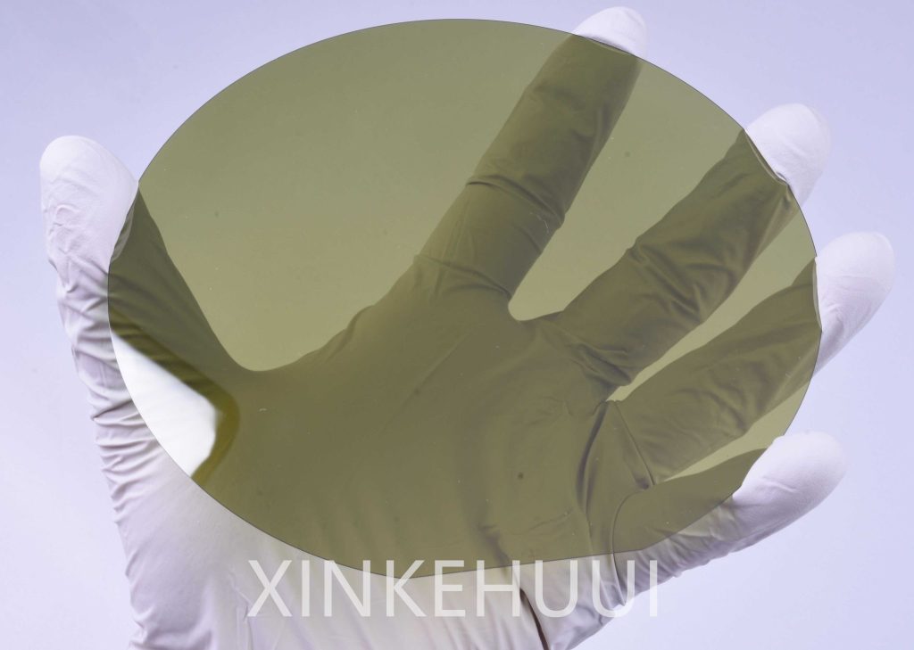
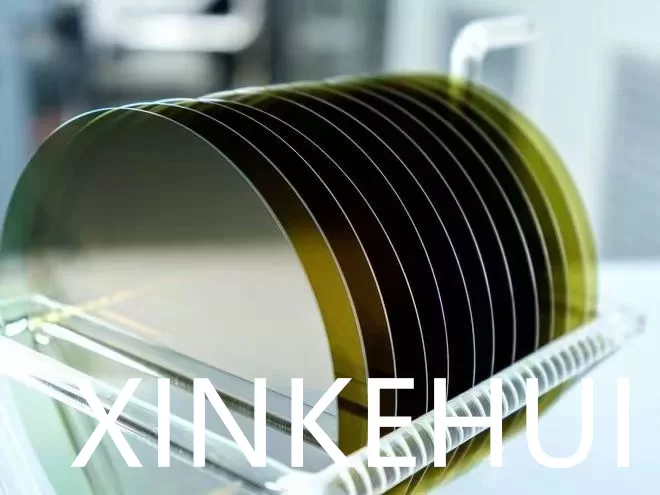
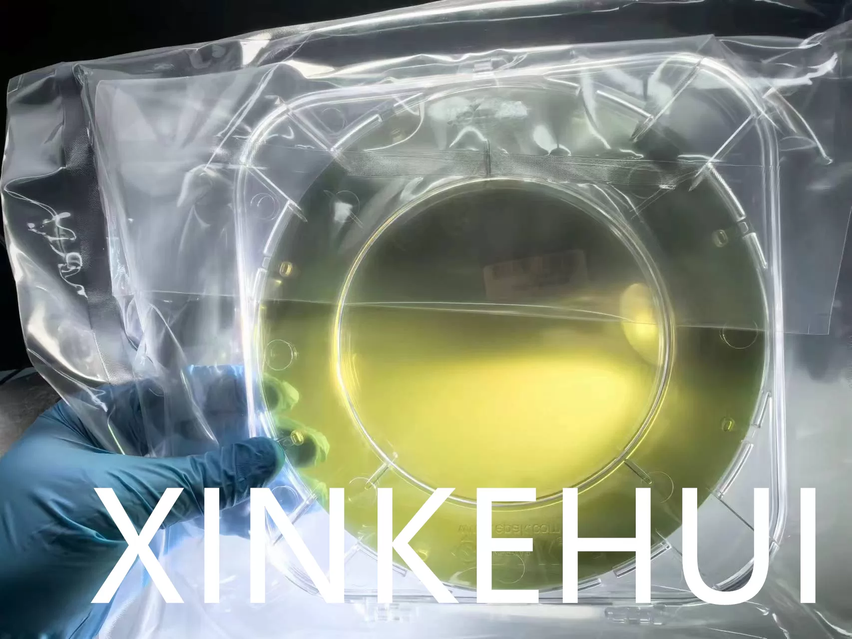
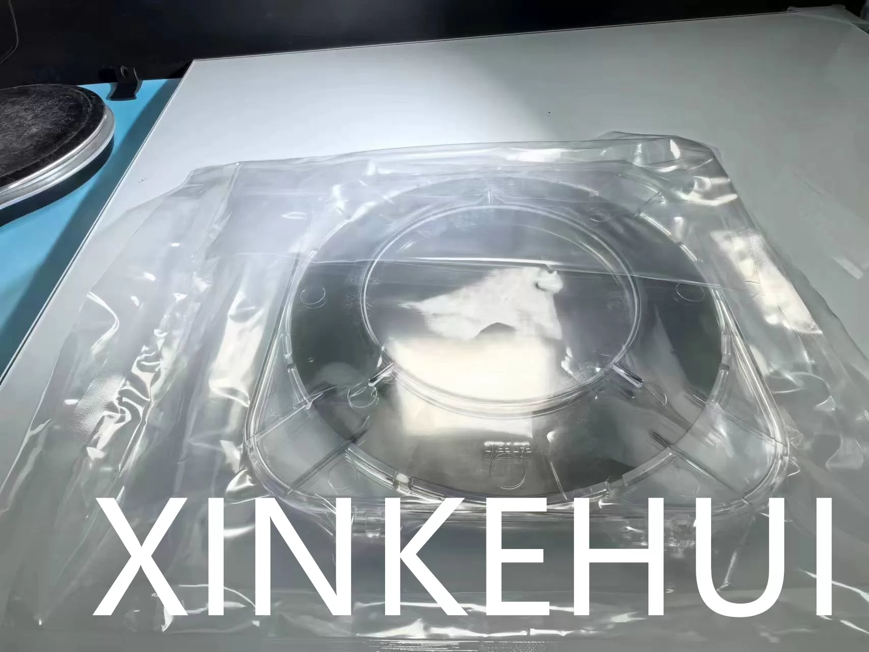
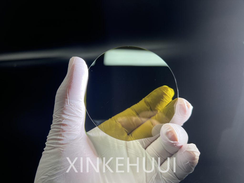
8inch Silicon Carbide Wafers‘ picture

8inch Silicon Carbide Wafers‘ properties
| Item | Specifications | |
|---|---|---|
| Polytype | 4H -SiC | 6H- SiC |
| Diameter | 2 inch | 3 inch | 4 inch | 6inch | 2 inch | 3 inch | 4 inch | 6inch |
| Thickness | 330 μm ~ 350 μm | 330 μm ~ 350 μm |
| Conductivity | N – type / Semi-insulating | N – type / Semi-insulating |
| Dopant | N2 ( Nitrogen )V ( Vanadium ) | N2 ( Nitrogen ) V ( Vanadium ) |
| Orientation | On axis <0001> Off axis <0001> off 4° | On axis <0001> Off axis <0001> off 4° |
| Resistivity | 0.015 ~ 0.03 ohm-cm (4H-N) | 0.02 ~ 0.1 ohm-cm (6H-N) |
| Micropipe Density(MPD) | ≤10/cm2 ~ ≤1/cm2 | ≤10/cm2 ~ ≤1/cm2 |
| TTV | ≤ 15 μm | ≤ 15 μm |
| Bow / Warp | ≤25 μm | ≤25 μm |
| Surface | DSP/SSP | DSP/SSP |
| Grade | Production / Research grade | Production / Research grade |
| Crystal Stacking Sequence | ABCB | ABCABC |
| Lattice parameter | a=3.076A , c=10.053A | a=3.073A , c=15.117A |
| Eg/eV(Band-gap) | 3.27 eV | 3.02 eV |
| ε(Dielectric Constant) | 9.6 | 9.66 |
| Refraction Index | n0 =2.719 ne =2.777 | n0 =2.707 , ne =2.755 |
Silicon carbide (SiC) wafers are semiconductor substrates made from crystalline silicon carbide, a compound of silicon and carbon. They are valued for their unique properties, which make them suitable for various high-performance electronic and optoelectronic applications. Here are some key properties of silicon carbide wafers:
- Wide Bandgap: Silicon carbide has a wide bandgap compared to silicon, which allows it to operate at higher temperatures and voltages. The bandgap of SiC is approximately 3 times larger than that of silicon, making it ideal for high-power, high-frequency, and high-temperature applications.
- High Thermal Conductivity: 8inch Silicon Carbide Wafers wafer has excellent thermal conductivity, which allows for efficient heat dissipation. This property enables SiC devices to handle higher power densities and operate at elevated temperatures without significant degradation in performance.
- High Electron Mobility: 8inch Silicon Carbide Wafers exhibits high electron mobility, which is beneficial for high-frequency and high-power applications. This high mobility results in faster switching speeds and lower on-resistance in SiC-based devices, leading to improved efficiency and performance.
- Chemical Stability: 8inch Silicon Carbide Wafers is chemically inert and can withstand harsh environments, including corrosive atmospheres and extreme temperatures. This property enhances the reliability and durability of SiC-based devices, making them suitable for demanding applications in aerospace, automotive, and industrial sectors.
- Mechanical Strength: 8inch Silicon Carbide Wafers are mechanically robust and exhibit high hardness and stiffness. This mechanical strength makes them less susceptible to mechanical damage and allows for the fabrication of thinner and lighter devices compared to traditional silicon substrates.
- Optical Transparency: 8inch Silicon Carbide Wafers is transparent in the infrared region, making it useful for optoelectronic applications such as infrared detectors and sensors.
- Low Power Losses: 8inch Silicon Carbide Wafers wafer devices have lower switching losses compared to silicon-based counterparts, resulting in higher efficiency and reduced power dissipation in power electronics applications.
Overall, the combination of these properties makes silicon carbide wafers highly desirable for a wide range of applications, including power electronics, RF/microwave devices, LED lighting, solar inverters, and electric vehicles.
8inch Silicon Carbide Wafers‘ advantage
ere are some additional benefits of using 8-inch silicon carbide (SiC) wafers:
- Enhanced Hardness: The high hardness of8inch Silicon Carbide Wafers provides durability and resistance to mechanical wear and damage, ensuring long-term reliability in harsh operating conditions.
- Improved Electrical Conductivity: The combination of high hardness and thermal conductivity in 8inch Silicon Carbide Wafers enhances their electrical conductivity, facilitating better performance in high-speed, high-temperature, and high-voltage applications.
- Miniaturization: 8inch Silicon Carbide Wafers’ high thermal conductivity enables efficient heat dissipation, allowing for the design of smaller and more compact devices without compromising performance. This supports the trend towards miniaturization in electronic devices.
- Low Coefficient of Thermal Expansion (CTE): The low CTE of SiC wafers ensures minimal dimensional changes with temperature fluctuations, enabling precise alignment and integration into electronic systems. This property is crucial for achieving high device yields and reliability.
- High Resistance to Thermal Shock:8inch Silicon Carbide Wafers’ ability to withstand rapid temperature changes without cracking or breaking improves manufacturing yield and device reliability, especially in environments with fluctuating temperatures.
- Chemical Inertness: 8inch Silicon Carbide Wafers’ resistance to chemical reactions with acids, alkalis, and molten salts up to 800°C expands their versatility in various applications and ensures stability in corrosive environments.
- High-Temperature Operation: The exceptional strength of 8inch Silicon Carbide Wafers at temperatures exceeding 1600°C enables their use in demanding high-temperature applications, such as aerospace, automotive, and industrial processes, where traditional silicon substrates may fail.
- Versatility: The combination of these advantages makes8inch Silicon Carbide Wafers suitable for a wide range of applications, including power electronics, RF/microwave devices, optoelectronics, and sensors, where superior performance, reliability, and durability are essential.
How are silicon carbide switches utilized in the field of power electronics?
Silicon carbide (SiC) is a material renowned for its myriad properties that find extensive utility in the realm of power electronics. With a bandgap larger than that of silicon and a dielectric breakdown strength surpassing both silicon and germanium, 8inch Silicon Carbide Wafers wafer stands out as an ideal candidate for power electronics applications. Its low specific on-resistance and formidable blocking voltage enable it to effortlessly handle high voltages over shorter distances within a device, leading to minimized power losses and diminished electrical resistance.
8inch Silicon Carbide Wafers switches represent highly efficient, high-voltage semiconductors capable of accommodating elevated voltages and frequencies without sacrificing performance. Their ability to be fashioned into smaller and lighter configurations compared to conventional silicon devices, coupled with their impressive thermal conductivity, renders them particularly well-suited for power applications, where the imperative lies in mitigating switching losses. Moreover, SiC switches boast a prolonged lifespan and exceptional durability, exemplified by products like Toshiba’s 650-V SiC MOSFET, renowned for its low ON-resistance and swift switching capabilities.
The intrinsic characteristics of SiC, characterized by low ON-resistance and a high bandgap, make it an optimal choice for power applications, offering superior efficiency, reduced size, and lower power consumption. These attributes not only facilitate a reduction in overall system dimensions but also extend their applicability to diverse realms, including solar inverters and industrial machinery. Furthermore, SiC’s durability, underscored by its high thermal conductivity and low ON-resistance, ensures resilience in the face of elevated temperatures, thereby enhancing reliability in power electronics applications.
In essence, while SiC garners acclaim for its utility in electrical and optical applications, its switches’ allure lies predominantly in their capacity to handle higher voltages and frequencies. In addition to their durability, SiC switches boast lightweight construction and minimal thermal resistance, which, when combined with their silicon counterparts, confer distinct advantages over traditional silicon. Their ability to operate within wide temperature ranges and exhibit low inductance serve to diminish switching losses and elevate system efficiency, rendering 8inch Silicon Carbide Wafers a favored choice in the realm of power electronics.
Despite its higher cost relative to silicon, 8inch Silicon Carbide Wafers offers myriad advantages over conventional materials, owing to its enhanced electrical conductivity, lower ON-resistance, and diminished total gate charge, all of which contribute to heightened power density and expedited switching speeds. Such attributes are pivotal in enhancing the efficacy of power electronics, particularly in scenarios where thermal stress poses a challenge. With its inherent properties, silicon carbide emerges as a versatile material with multifaceted applications across diverse domains.
In its essence, silicon carbide, a compound of carbon and silicon, possesses intrinsic insulating properties. However, through the introduction of impurities, it can be transformed into a semiconductor, rendering it a highly reliable and adaptable material for switches. Beyond its prowess in power electronics, silicon carbide power modules boast superior voltage handling capabilities, diminished switching losses, and refined thermal management, making them indispensable across a spectrum of applications, including high-speed switching and compact device integration.
What Is a SiC Wafer?
Silicon carbide (SiC) wafers serve as pivotal semiconductor materials with a rich history dating back to their development in 1893. Renowned for their versatility, 8inch Silicon Carbide Wafers find application in a multitude of electronic components, including Schottky diodes, Junction Barrier Schottky diodes, switches, and metal oxide semiconductor field-effect transistors (MOSFETs). The inherent high hardness of SiC renders it particularly well-suited for power electronic components, ensuring durability and longevity.
In the contemporary semiconductor landscape, the burgeoning demand for SiC semiconductors underscores the critical importance of wafer supply. Chipmakers are actively diversifying their sources, leveraging both in-house production capabilities and external suppliers to meet escalating market demands. This strategic approach not only fosters economies of scale but also serves to optimize production costs, driving industry growth and innovation.
8inch Silicon Carbide Wafers primarily manifest in two main types: polished wafers and epitaxial crystalline silicon carbide wafers. Polished wafers comprise single SiC discs crafted from high-purity SiC crystals, available in diameters ranging from 100mm to 150mm. These wafers find application in high-power electronics due to their exceptional quality and reliability. Epitaxial crystalline silicon carbide wafers, on the other hand, are produced through the meticulous layering of single SiC crystals onto a substrate surface, a process known as n-type epitaxy. This method demands precise control over material thickness and is favored for its versatility and versatility in various applications.
Furthermore, advancements in SiC technology have led to the development of beta silicon carbide, characterized by its hexagonal crystal structure akin to Wurtzite. Beta SiC, produced at temperatures exceeding 1700 degrees Celsius, holds promise for applications such as power semiconductors in electric vehicles. Several third-party SiC wafer suppliers are actively exploring the potential of this innovative material, heralding a new era of semiconductor manufacturing.
8inch Silicon Carbide Wafers epitomize high-performance semiconductor materials distinguished by exceptional electrical and thermal properties. Their superior thermal resistance and hardness render them indispensable across a spectrum of applications, spanning from power electronics to optical devices. Manufacturers such as MSE Supplies offer a diverse array of high-quality SiC wafers and substrates, catering to the burgeoning demand for advanced semiconductor solutions.
Despite their high cost and the requisite investment in modules, packaging, and silicon components, SiC devices continue to gain traction owing to their superior performance and efficiency. As manufacturers navigate the complex semiconductor landscape, adherence to precise specifications and cost considerations remains paramount. This necessitates a strategic approach informed by market dynamics and manufacturing capabilities, ensuring sustained growth and competitiveness in the ever-evolving semiconductor industry.
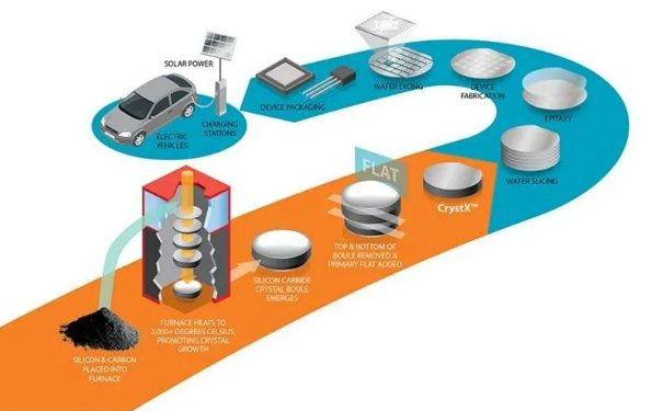
How 8inch Silicon Carbide Wafers Are Made
The manufacturing process of 8-inch silicon carbide (SiC) wafers involves several critical steps to ensure their quality and suitability for semiconductor applications.
- Batch Lapping: Once a boule of SiC crystal is grown into individual wafers, they are loaded into a batch lapping system. This system reduces the thickness of the wafers and ensures that the top and bottom surfaces are parallel. Each wafer is then manually unloaded, measured, and sorted according to thickness.
- Surface Preparation: Surface preparation is crucial to fabricating high-quality SiC wafers. To achieve the desired surface hardness, oxidation of the silicon wafer is performed. Additionally, the density of dislocations and scratches must be kept below a certain level to meet quality standards. If the surface is too rough, a wire saw is used to roughen it, although this process is labor-intensive and costly.
- Wafer Reclaim Process: X-Trinsic offers a wafer reclaim process, where the damaged surface layer of a wafer is removed and repolished to restore it to a device-ready state. This process can save costs for companies and increase the yield of a given wafer by up to 50%.
- Batch Processing: Current production of SiC wafers is typically done using batch processing tools, which have a lower throughput and are limited to smaller wafers. However, as the industry moves towards larger wafer sizes, batch processing tools may need to adapt to accommodate larger wafers efficiently.
- Defect Inspection and Removal: During the manufacturing process, SiC crystals are checked for dislocations and defects. Defective areas are identified, and any defects are removed to ensure the overall performance and quality of the semiconductor wafers.
- Purity and Epitaxial Film Processing: After the silicon substrate is manufactured, it undergoes processing to ensure the highest purity possible. Proper processing is essential to avoid creating defects in the epitaxial film, resulting in better-quality and more efficient wafers that can be tailored to specific requirements.
Overall, the manufacturing process of 8-inch SiC wafers involves a series of precise steps to produce high-quality semiconductor materials suitable for a range of applications.
Recommendations for similar products
4H N-TYPE SIC SUBSTRATE Ideal High-Temperature Stable Materials
The 4H N-Type Silicon Carbide (SiC) Substrate stands at the forefront of semiconductor technology, embodying a range of superior attributes that propel electronic applications into new frontiers. This product overview explores the fundamental characteristics, diverse applications, and inherent advantages that define the 4H N-Type 8inch Silicon Carbide Wafers Substrate, elucidating its pivotal role in advancing high-performance semiconductor devices.
The key characteristics of the 4H N-Type Silicon Carbide (SiC) Substrate define its exceptional role in semiconductor technology, setting it apart as a pioneering material with attributes that redefine the landscape of electronic applications. This in-depth exploration unveils the multifaceted nature of the substrate, shedding light on its fundamental properties that underpin its significance in the realm of high-performance semiconductor devices.
SiC Substrate Providing an Ideal Solution for New Energy Vehicles
Silicon Carbide (SiC) substrates represent a pivotal class of materials in the realm of electronic and semiconductor industries. Renowned for their exceptional physical and electrical properties, SiC substrates have found diverse applications across various technological domains. This abstract delves into the different types of SiC substrates, their unique characteristics, and their wide-ranging applications.
The 4H n-type Silicon Carbide substrate stands at the forefront of modern semiconductor technology, influencing a multitude of applications that require high-performance electronic components. From powering electronic devices to enhancing communication systems and enabling renewable energy technologies, the versatility of 4H n-type SiC substrates continues to drive innovation across diverse industries.