
In the rapidly evolving landscape of high-performance computing (HPC), we are witnessing a transition from the era of “Silicon for everything” to an era of “Specialized Materials for Performance.” As NVIDIA prepares to unleash its next-generation Rubin architecture, a quiet but seismic shift is happening beneath the silicon dies. To overcome the physical limits of current AI chip performance, NVIDIA is reportedly planning to replace traditional silicon intermediate substrates in the CoWoS (Chip on Wafer on Substrate) advanced packaging process with Silicon Carbide (SiC).
This move marks a pivotal moment for the semiconductor industry. For years, SiC was the “heavyweight workhorse” of the power electronics world—powering electric vehicle (EV) inverters and renewable energy grids . Now, it is entering the heart of the data center to solve the most pressing crisis in AI: the “Thermal Wall.”
The Crisis: Why Silicon Interposers are Hitting a Thermal Bottleneck
The relentless pursuit of AI compute power has pushed GPU power consumption through the ceiling. NVIDIA’s H100 GPU already consumes roughly $700 \text{ W}$, and the upcoming Rubin processors are expected to exceed a staggering $1000 \text{ W}$. At these levels, the traditional silicon interposer—the bridge that connects the GPU logic and High Bandwidth Memory (HBM)—has become a liability.
1. Thermal Conductivity Limitations
Silicon has a thermal conductivity of approximately $150 \text{ W/mK}$. While this was sufficient for previous generations, it cannot effectively dissipate the intense heat flux generated by thousand-watt AI chips. Inefficient heat dissipation leads to “thermal throttling,” where the chip must reduce its clock speed to prevent physical damage, effectively erasing the performance gains of the $3 \text{ nm}$ or $2 \text{ nm}$ nodes.
2. The Coefficient of Thermal Expansion (CTE) Mismatch
Reliability in advanced packaging depends on how materials expand and contract. While silicon interposers have a CTE of $4.2 \text{ ppm/}^\circ\text{C}$, the surrounding package components and the extreme heat cycles of AI workloads can cause mechanical stress, leading to delamination or micro-cracks over time.
The SiC Solution: A 70% Reduction in Thermal Resistance
By switching to Silicon Carbide as the interposer material, NVIDIA and its manufacturing partner TSMC are leveraging a material with properties that perfectly match the requirements of 2.5D and 3D stacking.
The Physics of Performance
Silicon Carbide boasts a thermal conductivity of approximately $490 \text{ W/mK}$—more than three times that of silicon. In a high-heat-flux environment, this means heat is moved away from the core logic dies with unprecedented efficiency. Tests have shown that replacing silicon interposers with SiC can reduce thermal resistance by nearly 70%.2
For an AI data center operator, this translates into real-world gains:
- Lower Junction Temperatures: SiC interposers can lower the operating temperature of a flagship GPU from $95^\circ\text{C}$ to $75^\circ\text{C}$.
- Doubled Lifespan: By reducing thermal stress and operating temperatures, the physical lifespan of the chip can be extended by up to two times.
- Reduced Cooling Costs: Improved passive heat dissipation within the package can lower the cooling energy requirements of a data center by roughly 30%.
Implementation Roadmap: From Blackwell to Rubin Ultra
NVIDIA’s transition to SiC interposers is a carefully phased strategic move. According to the current roadmap, we will see the following progression:
- 2025–2026 (Blackwell and First-Gen Rubin): Flagship AI chips will continue to utilize silicon interposers (specifically the CoWoS-L variant) while TSMC and its partners finalize the SiC manufacturing supply chain.3
- 2027 (The SiC Breakthrough): This is the year targeted for the full-scale adoption of SiC interposers in NVIDIA’s high-end processors.3 This coincides with TSMC’s planned launch of a “7x-mask” CoWoS design, which will expand the interposer area to a massive $14,400 \text{ mm}^2$.
The Rise of the 12-Inch SiC Wafer Market
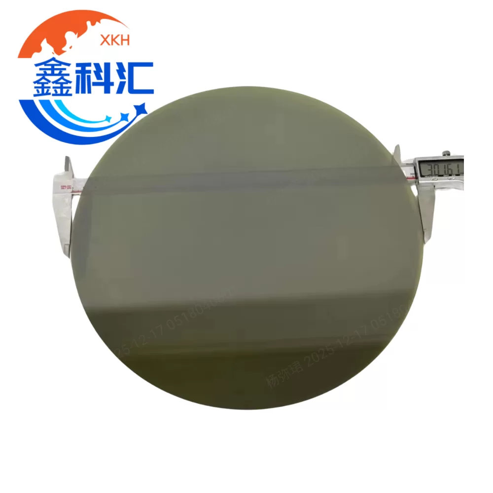
One of the most significant consequences of NVIDIA’s switch is the explosion in SiC substrate demand.1 Historically, the SiC industry has focused on $6\text{-inch}$ and $8\text{-inch}$ wafers for the automotive sector. However, to meet the requirements of advanced packaging interposers, the industry is shifting toward $12\text{-inch}$ ($300 \text{ mm}$) SiC wafers.
Why 12-Inch?
- Integration Density: A $12\text{-inch}$ SiC substrate offers a 90% larger surface area than an $8\text{-inch}$ version. This is critical for NVIDIA’s “Scale-Up” strategy, where a single interposer must house multiple GPU chiplets and 8 to 12 HBM4 memory stacks.
- Cost Scaling: While $12\text{-inch}$ SiC substrates are currently expensive, the volume driven by the AI sector is expected to bring prices down to viable levels by 2027, similar to the historical price curve of silicon wafers.
- Reduced Defect Sensitivity: In power electronics, a single micropipe can ruin a MOSFET. However, when used as a thermal interposer, the material requirements for crystal integrity are slightly different. The focus shifts from electrical carrier mobility to phonon transmission (quantized lattice vibrations that conduct heat). This allows for a faster ramp-up of $12\text{-inch}$ production even as the industry perfects the crystal growth process.
Manufacturing Challenges: Precision at the Diamond Level
The transition to SiC is not without hurdles. Silicon Carbide’s hardness is approximately $9.2 \text{ Mohs}$—second only to diamond.3 This makes traditional wafer dicing and slicing extremely difficult.
If the cutting technology is inadequate, the SiC surface can develop “wave-like” irregularities that render it unusable for the high-precision bonding required in CoWoS packaging. To solve this, industry leaders are turning to advanced laser-assisted dicing and specialized multi-wire saw machines to achieve tolerances of $\pm 0.01 \text{ mm}$.
Strategic Positioning: How ZMSH Supports the AI Infrastructure
As a leading provider of advanced semiconductor materials, ZMSH (Shanghai Famous Trade Co., Ltd) is at the forefront of this material revolution. We understand that the future of AI depends on the stability and thermal performance of the substrate.
We specialize in the customization and supply of 2-12 inch conductive and semi-insulating Silicon Carbide (SiC) substrates, tailored for the most demanding applications in power electronics and AI packaging .
- Full Spectrum Customization: We offer tailored solutions for crystal orientation ($<100>$/$<111>$), varying resistivity levels ($10^{-3}$ to $10^{10} \Omega\cdot\text{cm}$), and thicknesses ranging from $350$ to $2000 \mu\text{m}$.
- Precision Machining: Utilizing our advanced machinery workshop, we provide end-to-end technical collaboration, including wafer slicing and surface finishing that ensures compatibility with next-generation high-temperature bonding requirements.3
- Reliable Global Supply: With a global sales network and a strict quality control system (certified by RoHS and Supplier Capability Assessments), we provide the reliable backbone needed for the AI supply chain .
Conclusion: SiC as the Cornerstone of Next-Gen Computing
The report that NVIDIA processors are switching to Silicon Carbide thermal interposers is more than a technical footnote; it is a declaration that the AI era requires a new material foundation. By overcoming the thermal bottleneck, SiC enables the “extreme scale-up” required for the next generation of reasoning AI models and “Agentic AI” platforms.
As we move toward 2027, the synergy between AI-driven demand and material innovation will position Silicon Carbide as the cornerstone of semiconductor infrastructure. For engineers and procurement specialists looking to navigate this transition, partnering with a supplier that offers both the material expertise and the precision manufacturing capability is essential.
Contact XINKEHUI today to explore how our 12-inch SiC substrate capabilities can power your next-generation high-performance computing projects.