
As the demand for high-efficiency power electronics continues to grow, Silicon Carbide (SiC) wafers have become a foundational material for next-generation semiconductor devices. Compared with conventional silicon substrates, SiC offers a wider bandgap, higher critical electric field strength, superior thermal conductivity, and better high-temperature performance. These characteristics make SiC indispensable in electric vehicles, renewable energy systems, industrial power modules, and high-frequency communication devices.
However, the advantages of SiC come with significant manufacturing challenges. Due to the extremely high crystal growth temperatures and complex lattice structure, SiC wafers are prone to various structural and surface defects during crystal growth, slicing, polishing, and epitaxial processing. These defects directly affect device reliability, yield, and electrical performance.
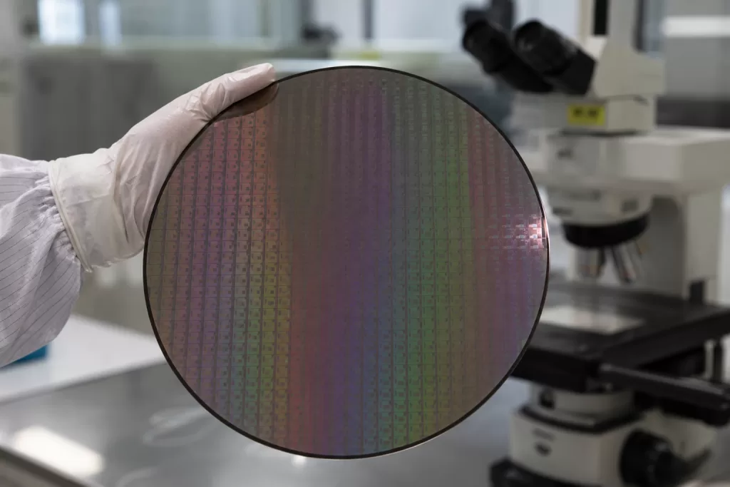
This article provides an academic overview of common defects found in SiC wafers and the inspection methods used to identify and characterize them.
Why Defect Control Matters in SiC Wafers
SiC single crystals are commonly produced using the Physical Vapor Transport (PVT) method. During crystal growth, fluctuations in temperature gradients, supersaturation, stress distribution, and impurity incorporation can introduce crystallographic imperfections.
Even a relatively low defect density may cause significant issues in power devices, including:
- Increased leakage current
- Reduced breakdown voltage
- Elevated on-resistance
- Device degradation during operation
- Lower manufacturing yield
For high-voltage and high-power applications, defect density has become one of the most critical parameters in SiC substrate qualification.
Common Defects in SiC Wafers
1. Micropipes
Micropipes are hollow-core crystallographic defects associated with screw dislocations and were historically considered one of the most severe defects in SiC substrates.
Characteristics:
- Tube-like hollow structure
- Diameter typically ranges from 0.1–10 μm
- Extends through the crystal growth direction
- Strong impact on high-voltage device performance
Micropipes can significantly reduce breakdown voltage because they create localized electric field concentration. Considerable progress has been made in reducing micropipe density in modern 4-inch and 6-inch SiC wafers, although stringent control remains necessary for advanced applications.
2. Threading Screw Dislocations (TSD)
Threading screw dislocations propagate along the crystal growth axis and are associated with spiral growth mechanisms.
Potential impacts include:
- Surface morphology irregularities
- Epitaxial step distortion
- Local electrical non-uniformity
These defects may influence epitaxial growth quality and introduce variability in device characteristics.
3. Basal Plane Dislocations (BPD)
Basal Plane Dislocations are among the most extensively studied defects in SiC power device technology.
Characteristics:
- Exist within the basal plane of the crystal
- Can transform during device operation
- Particularly problematic for bipolar devices
BPDs are linked to a phenomenon known as bipolar degradation, where stacking fault expansion under carrier injection gradually reduces device performance.
Consequences may include:
- Forward voltage drift
- Reduced device lifetime
- Performance instability
4. Stacking Faults
Stacking faults arise when the normal sequence of atomic layer stacking becomes disrupted.
In SiC materials, stacking faults may:
- Alter local electronic structures
- Influence carrier transport
- Degrade optical or electrical properties
Certain stacking faults can expand under electrical stress, making them especially important for long-term reliability studies.
5. Surface Scratches
Mechanical processing steps such as grinding, lapping, chemical mechanical polishing (CMP), and wafer handling can introduce scratches.
Typical characteristics:
- Linear surface marks
- Local roughness variation
- Surface reflectivity differences
Even shallow scratches can interfere with photolithography and epitaxial uniformity.
6. Particle Contamination
Particles may originate from:
- Polishing residue
- Environmental contamination
- Equipment wear
- Wafer transportation processes
Surface particles may cause:
- Patterning defects
- Epitaxial abnormalities
- Yield reduction
Because of these risks, SiC wafer production requires stringent cleanroom control.
7. Edge Chipping and Microcracks
During wafer slicing or edge grinding, mechanical stress may generate edge damage.
Examples include:
- Edge fractures
- Small chips
- Microcrack formation
These defects can reduce mechanical strength and increase wafer breakage risks during automated processing.
Inspection Methods for SiC Wafer Defects
Since different defect types exhibit different physical characteristics, multiple characterization techniques are often used together.
| Inspection Method | Primary Function | Typical Detectable Defects |
|---|---|---|
| Optical Microscopy | Surface observation | Scratches, particles, edge defects |
| Atomic Force Microscopy (AFM) | Nanometer-scale topography | Surface roughness |
| X-Ray Diffraction (XRD) | Crystal structure analysis | Lattice distortion |
| KOH Etching | Revealing dislocation sites | BPD, TSD |
| Photoluminescence (PL) Mapping | Defect imaging | Dislocations, micropipes |
| X-ray Topography (XRT) | Internal crystal inspection | Micropipes, stacking faults |
| Raman Spectroscopy | Stress and lattice evaluation | Structural abnormalities |
| Automated Optical Inspection (AOI) | Large-scale surface screening | Surface defects |
| Laser Scattering Inspection | Particle detection | Surface contamination |
Among these techniques, PL mapping and X-ray topography have become industry-standard approaches for large-area defect evaluation.
Typical SiC Wafer Inspection Workflow
A comprehensive SiC quality-control process usually involves several inspection stages:
Incoming substrate inspection → Surface characterization → Defect mapping → Crystal quality analysis → Epitaxy qualification → Final inspection
For advanced device fabrication, additional evaluations may include:
- Full-wafer PL mapping
- Defect density statistics
- Crystal orientation analysis
- Automated defect classification
These steps help improve process consistency and optimize downstream manufacturing.
Emerging Trends: AI-Based Defect Analysis
As SiC technology moves toward larger wafer diameters such as 8-inch substrates, conventional inspection approaches face limitations in throughput and complexity.
Recent developments increasingly integrate:
- Artificial intelligence image recognition
- Machine learning defect classification
- Automated defect prediction
- Full-process data correlation systems
Future inspection strategies are expected to evolve from defect detection toward predictive quality control.
Conclusion
Defect control remains one of the central challenges in SiC wafer technology. Structural defects such as micropipes, threading dislocations, basal plane dislocations, and stacking faults, together with surface imperfections and contamination, significantly influence semiconductor device performance.
Through advanced characterization techniques such as PL mapping, X-ray topography, KOH etching, and automated optical inspection, manufacturers can better evaluate substrate quality and improve device yield. As SiC continues to expand into high-power and high-reliability applications, more intelligent and precise inspection technologies will play an increasingly important role in the semiconductor industry.