
Popis
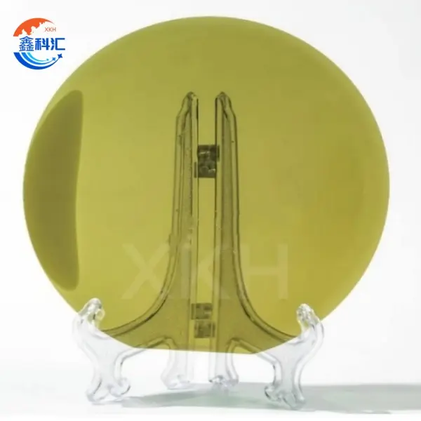
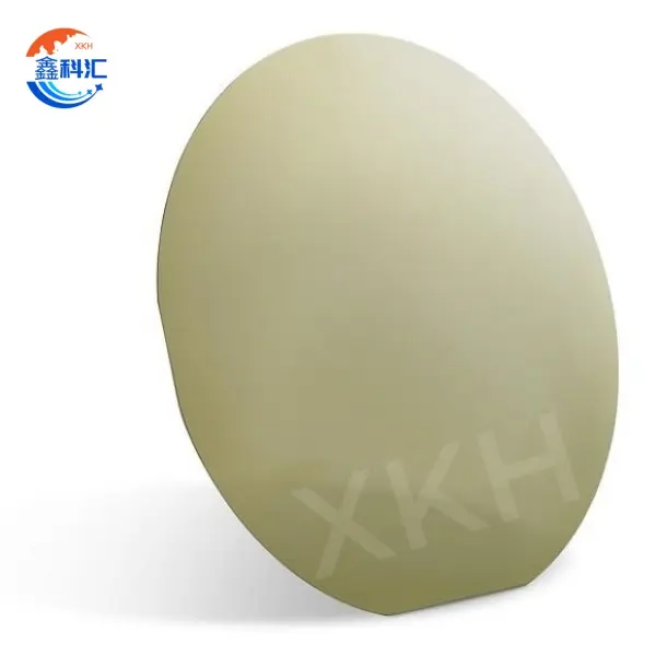
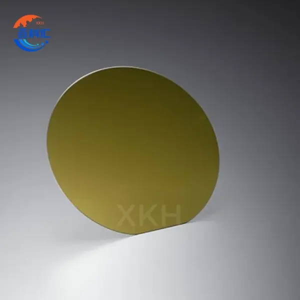
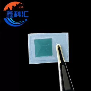
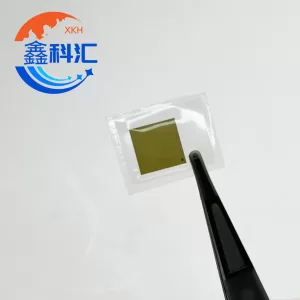
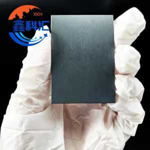
The 12-inch (300mm) silicon carbide substrate is a next-generation large-diameter wafer engineered for high-performance semiconductor manufacturing. Based on 4H-N SiC single-crystal technology, this prime-grade substrate offers exceptional electrical, thermal, and mechanical properties, making it ideal for high-power, high-frequency, and high-temperature device applications.
With the transition from 6-inch to 8-inch and now 12-inch platforms, SiC wafers significantly improve chip yield, lower cost per device, and accelerate mass production of power electronics.
| Parametr | ZeroMPD Production Grade (Z Grade) | Standard Production Grade (P Grade) | Dummy Grade (D Grade) |
|---|---|---|---|
| Průměr | 300 mm | 300 mm | 300 mm |
| Tloušťka | 750μm ± 15μm | 750μm ± 25μm | 750μm ± 25μm |
| Orientace destičky | Off axis: 4.0° towards <1120> ±0.5° for 4H-N | On axis: <0001> ±0.5° for 4H-SI | — |
| Micropipe Density (MPD) | 4H-N: ≤0.4 cm⁻²; 4H-SI: ≤5 cm⁻² | 4H-N: ≤4 cm⁻²; 4H-SI: ≤10 cm⁻² | 4H-N: ≤25 cm⁻²; 4H-SI: ≤25 cm⁻² |
| Odolnost | 4H-N: 0.015 ~ 0.024 Ω·cm | 4H-N: 0.015 ~ 0.028 Ω·cm | 4H-SI: ≥1E10 Ω·cm; 4H-SI: ≥1E5 Ω·cm |
| Primary Flat Orientation | {10-10} ±5.0° | {10-10} ±5.0° | {10-10} ±5.0° |
| Primární délka bytu | N/A | Notch | Notch |
| Edge Exclusion | 3 mm | 3 mm | 3 mm |
| LTV/TTV/Bow/Warp | ≤5μm/ ≤15μm/ ≤35μm/ ≤55μm | ≤5μm/ ≤15μm/ ≤35μm/ ≤55μm | ≤5μm/ ≤15μm/ ≤35μm/ ≤55μm |
| Drsnost | Polish Ra ≤1 nm; CMP Ra ≤0.2 nm | Ra ≤0.5 nm | Ra ≤0.5 nm |
| Edge Cracks by High Intensity Light | Žádné | Žádné | Cumulative length ≤ 20 mm, single length ≤ 2 mm |
| Hex Plates by High Intensity Light | Žádné | Žádné | Cumulative area ≤ 0.1% |
| Polytype Areas by High Intensity Light | Žádné | Žádné | Cumulative area ≤ 3% |
| Visual Carbon Inclusions | Žádné | Žádné | Cumulative area ≤ 3% |
| Silicon Surface Scratches | Žádné | Žádné | Cumulative length ≤ 1 × wafer diameter |
| Edge Chips by High Intensity Light | None permitted ≥0.2mm width and depth | 7 allowed, ≤1 mm each | 7 allowed, ≤1 mm each |
| Threading Screw Dislocation (TSD) | ≤500 cm⁻² | N/A | N/A |
| Base Plane Dislocation (BPD) | ≤1000 cm⁻² | N/A | N/A |
| Silicon Surface Contamination by High Intensity Light | Žádné | Žádné | Žádné |
| Packaging | Multi-wafer cassette or single wafer container | Multi-wafer cassette or single wafer container | Multi-wafer cassette or single wafer container |
Klíčové vlastnosti
● Superior Thermal Management
SiC provides thermal conductivity over three times that of silicon, enabling efficient heat dissipation in high-power systems such as EV inverters and industrial converters.
● High Breakdown Electric Field
The breakdown field strength of 4H-SiC is nearly an order of magnitude higher than silicon, supporting high-voltage and high-reliability applications.
● Wide Bandgap Energy (3.26 eV)
A broad bandgap enables stable operation under high temperature, high frequency, and harsh environmental conditions.
● Outstanding Mechanical Properties
Mohs hardness of 9.2 offers excellent wear resistance and mechanical robustness during device processing.
● Chemical & Thermal Stability
SiC maintains structural and electrical stability in corrosive, high-temperature, and high-stress manufacturing environments.
● Large-Diameter Growth Technology
Prime-grade 12-inch (300mm) wafers help customers increase throughput, optimize device design, and reduce long-term production costs.
● Low Defect Density
Advanced crystal growth and wafering technologies ensure uniformity, high epitaxial compatibility, and stable device performance.
Main Application Areas
1. Power Electronics
SiC MOSFETy for EV traction inverters, industrial drives, PV inverters
Schottky Barrier Diodes (SBDs) for high-efficiency rectification
Power modules operating in high-voltage and high-current environments
2. RF & Microwave Devices
RF power amplifiers for Základnové stanice 5G
Microwave devices for radar, satellite communication, and phased-array systems
3. New Energy Vehicles
Palubní nabíječky (OBC)
Fast-charging power conversion modules
High-efficiency traction system components
4. Industrial & Energy Infrastructure
Smart grid HVDC systems
High-voltage inverters and power control equipment
Industrial automation & robotics
5. Aerospace & Harsh-Environment Electronics
Vysokoteplotní elektronika
Radiation-resistant and extreme-environment devices
6. Scientific Research
Wide bandgap semiconductor device R&D
Advanced epitaxy, doping, and material characterization
Why Choose Our 12-Inch SiC Substrate?
● Customized Manufacturing
Various crystal orientations, resistivities, surface finish levels (CMP, epi-ready), and wafer thickness options are available.
● Process Integration Support
Technical guidance for epitaxy, lithography, doping, thinning, and device fabrication ensures seamless production compatibility.
● Comprehensive Quality Assurance
Strict defect inspection including:
Micropipe analysis
BPD/TSD mapping
Surface particle monitoring
Flatness and uniformity measurements
● R&D Partnership
We work closely with customers on new device structures, large-diameter wafer development, and next-generation SiC technology innovation.
The 12-inch 4H-N silicon carbide substrate represents a major milestone in the evolution of wide bandgap semiconductors. Its superior thermal conductivity, high breakdown strength, and large-size platform make it a core material for future high-power and high-efficiency electronic systems.
Whether for electric vehicles, power grids, RF systems, or aerospace, 300mm SiC wafers deliver performance, scalability, and reliability for next-generation semiconductor manufacturing.

Recenze
Zatím zde nejsou žádné recenze.