
描述
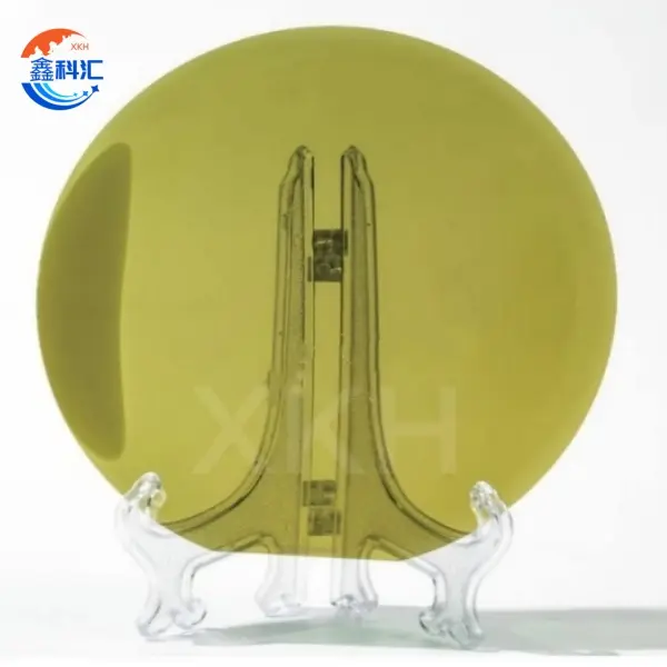
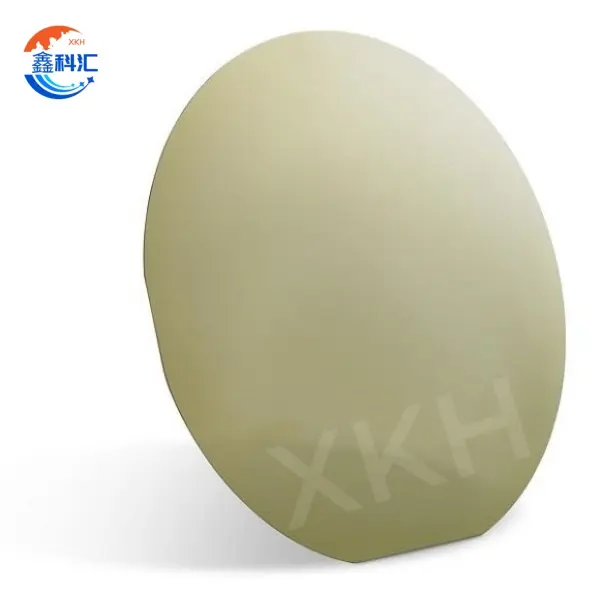
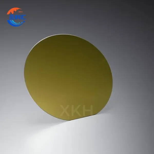
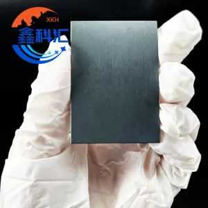
Das 12-Zoll-Siliziumkarbid-Substrat (300 mm) ist ein Wafer der nächsten Generation mit großem Durchmesser, der für die Hochleistungs-Halbleiterfertigung entwickelt wurde. Basierend auf der 4H-N SiC-Einkristalltechnologie bietet dieses erstklassige Substrat außergewöhnliche elektrische, thermische und mechanische Eigenschaften, die es ideal für Anwendungen mit hoher Leistung, hohen Frequenzen und hohen Temperaturen machen.
With the transition from 6-inch to 8-inch and now 12-inch platforms, SiC wafers significantly improve chip yield, lower cost per device, and accelerate mass production of power electronics.
| Parameter | ZeroMPD Production Grade (Z Grade) | Standard Production Grade (P Grade) | Dummy Grade (D Grade) |
|---|---|---|---|
| Durchmesser | 300 mm | 300 mm | 300 mm |
| Dicke | 750μm ± 15μm | 750μm ± 25μm | 750μm ± 25μm |
| Wafer-Ausrichtung | Off axis: 4.0° towards <1120> ±0.5° for 4H-N | On axis: <0001> ±0.5° for 4H-SI | — |
| Micropipe Density (MPD) | 4H-N: ≤0.4 cm⁻²; 4H-SI: ≤5 cm⁻² | 4H-N: ≤4 cm⁻²; 4H-SI: ≤10 cm⁻² | 4H-N: ≤25 cm⁻²; 4H-SI: ≤25 cm⁻² |
| Widerstandsfähigkeit | 4H-N: 0.015 ~ 0.024 Ω·cm | 4H-N: 0.015 ~ 0.028 Ω·cm | 4H-SI: ≥1E10 Ω·cm; 4H-SI: ≥1E5 Ω·cm |
| Primary Flat Orientation | {10-10} ±5.0° | {10-10} ±5.0° | {10-10} ±5.0° |
| Primäre Wohnung Länge | N/A | Notch | Notch |
| Ausschluss von Kanten | 3 mm | 3 mm | 3 mm |
| LTV/TTV/Bow/Warp | ≤5μm/ ≤15μm/ ≤35μm/ ≤55μm | ≤5μm/ ≤15μm/ ≤35μm/ ≤55μm | ≤5μm/ ≤15μm/ ≤35μm/ ≤55μm |
| Rauhigkeit | Polish Ra ≤1 nm; CMP Ra ≤0.2 nm | Ra ≤0.5 nm | Ra ≤0.5 nm |
| Edge Cracks by High Intensity Light | Keine | Keine | Cumulative length ≤ 20 mm, single length ≤ 2 mm |
| Hex Plates by High Intensity Light | Keine | Keine | Cumulative area ≤ 0.1% |
| Polytype Areas by High Intensity Light | Keine | Keine | Cumulative area ≤ 3% |
| Visual Carbon Inclusions | Keine | Keine | Cumulative area ≤ 3% |
| Silicon Surface Scratches | Keine | Keine | Cumulative length ≤ 1 × wafer diameter |
| Edge Chips by High Intensity Light | None permitted ≥0.2mm width and depth | 7 allowed, ≤1 mm each | 7 allowed, ≤1 mm each |
| Threading Screw Dislocation (TSD) | ≤500 cm⁻² | N/A | N/A |
| Base Plane Dislocation (BPD) | ≤1000 cm⁻² | N/A | N/A |
| Silicon Surface Contamination by High Intensity Light | Keine | Keine | Keine |
| Packaging | Multi-wafer cassette or single wafer container | Multi-wafer cassette or single wafer container | Multi-wafer cassette or single wafer container |
Wesentliche Merkmale
● Superior Thermal Management
SiC provides thermal conductivity over three times that of silicon, enabling efficient heat dissipation in high-power systems such as EV inverters and industrial converters.
● High Breakdown Electric Field
The breakdown field strength of 4H-SiC is nearly an order of magnitude higher than silicon, supporting high-voltage and high-reliability applications.
● Wide Bandgap Energy (3.26 eV)
A broad bandgap enables stable operation under high temperature, high frequency, and harsh environmental conditions.
● Outstanding Mechanical Properties
Mohs hardness of 9.2 offers excellent wear resistance and mechanical robustness during device processing.
● Chemical & Thermal Stability
SiC maintains structural and electrical stability in corrosive, high-temperature, and high-stress manufacturing environments.
● Large-Diameter Growth Technology
Prime-grade 12-inch (300mm) wafers help customers increase throughput, optimize device design, and reduce long-term production costs.
● Low Defect Density
Advanced crystal growth and wafering technologies ensure uniformity, high epitaxial compatibility, and stable device performance.
Main Application Areas
1. Power Electronics
SiC-MOSFETs for EV traction inverters, industrial drives, PV inverters
Schottky Barrier Diodes (SBDs) for high-efficiency rectification
Power modules operating in high-voltage and high-current environments
2. RF & Microwave Devices
RF power amplifiers for 5G base stations
Microwave devices for radar, satellite communication, and phased-array systems
3. New Energy Vehicles
On-board chargers (OBC)
Fast-charging power conversion modules
High-efficiency traction system components
4. Industrial & Energy Infrastructure
Smart grid HVDC systems
High-voltage inverters and power control equipment
Industrial automation & robotics
5. Aerospace & Harsh-Environment Electronics
Hochtemperaturelektronik
Radiation-resistant and extreme-environment devices
6. Scientific Research
Wide bandgap semiconductor device R&D
Advanced epitaxy, doping, and material characterization
Why Choose Our 12-Inch SiC Substrate?
● Customized Manufacturing
Various crystal orientations, resistivities, surface finish levels (CMP, epi-ready), and wafer thickness options are available.
● Process Integration Support
Technical guidance for epitaxy, lithography, doping, thinning, and device fabrication ensures seamless production compatibility.
● Comprehensive Quality Assurance
Strict defect inspection including:
Micropipe analysis
BPD/TSD mapping
Surface particle monitoring
Flatness and uniformity measurements
● R&D Partnership
We work closely with customers on new device structures, large-diameter wafer development, and next-generation SiC technology innovation.
The 12-inch 4H-N silicon carbide substrate represents a major milestone in the evolution of wide bandgap semiconductors. Its superior thermal conductivity, high breakdown strength, and large-size platform make it a core material for future high-power and high-efficiency electronic systems.
Whether for electric vehicles, power grids, RF systems, or aerospace, 300mm SiC wafers deliver performance, scalability, and reliability for next-generation semiconductor manufacturing.

Rezensionen
Es gibt noch keine Rezensionen.