
Silicon carbide (SiC) has rapidly become one of the most critical materials in modern semiconductor technology. As industries shift toward high-efficiency power electronics, electric vehicles (EVs), renewable energy systems, and high-frequency devices, the demand for high-quality SiC wafers continues to surge.
However, one reality remains clear:
the more complex the SiC process, the more critical advanced manufacturing technology becomes.
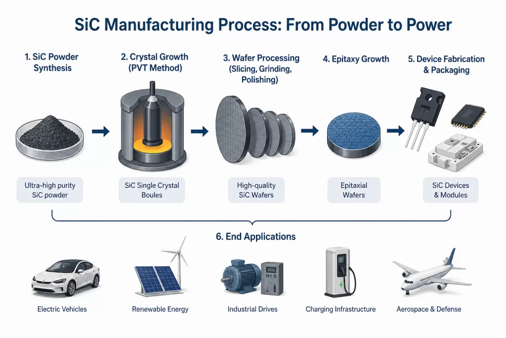
The SiC Industry Value Chain: From Powder to Power Devices
The silicon carbide industry consists of three key stages:
1. Upstream: Substrate & Epitaxy
- High-purity SiC powder synthesis
- Crystal growth (boule formation)
- Wafer slicing, grinding, and polishing
- Epitaxial layer deposition
2. Midstream: Device Fabrication
- Photolithography
- Ion implantation
- Etching and deposition
- Device integration
3. Downstream: End Applications
- Elektrická vozidla (napájecí moduly pro elektromobily)
- Renewable energy inverters
- Pohony průmyslových motorů
- Aerospace and high-radiation environments
Ultra-High Purity SiC Powder: The Foundation of Crystal Quality
The quality of SiC destičky starts with the powder.
For single crystal growth, purity levels must reach 99.95% to 99.9999%.
Main Synthesis Methods
1. Chemical Vapor Deposition (CVD)
- Produces ultra-fine, high-purity powders
- Excellent control over impurities
- Limitation: high cost, low throughput
2. Sol-Gel Method (Liquid Phase)
- High uniformity at molecular level
- Suitable for ultra-fine powders
- Complex process control
3. Improved Self-Propagating High-Temperature Synthesis (SHS)
- Widely used in industry
- Temperature range: 1400°C – 2000°C
- Výhody:
- Fast production
- Lower cost
- High scalability
In practice, powder purification is essential before crystal growth to remove impurities such as Al, B, and free silicon.
SiC Crystal Growth Technologies: The Core Barrier
Crystal growth is the most technically demanding step in SiC manufacturing.
Physical Vapor Transport (PVT) – Industry Standard
- Dominant method for bulk SiC crystal growth
- Enables large-diameter substrates
- Proces:
- Sublimation of SiC source material
- Vapor transport to seed crystal
- Controlled recrystallization
Pros:
- High crystal quality
- Scalable for mass production
Cons:
- Slow growth rate
- High energy consumption
- Expensive equipment
Chemical Vapor Deposition (CVD) – Precision Growth
- Used mainly for epitaxial layers
- Excellent thickness and uniformity control
Pros:
- High-quality films
- Precise doping control
Cons:
- High cost
- Complex system requirements
Liquid Phase Growth (LPE) – Niche Application
- Growth in high-temperature molten solution
Omezení:
- Small wafer size
- Lower thermal stability
- Limited industrial adoption
Wafer Processing: The Key to Cost Reduction
Even with high-quality crystals, wafer processing determines final yield and cost.
1. Wafer Slicing
Laser Cutting
- High precision
- Suitable for complex geometries
Wire Saw Cutting
- Better for thick substrates
- Lower precision than laser
2. Grinding and Polishing
The process includes:
- Coarse Grinding
- Removes damage layer
- Abrasives: Al₂O₃, SiC
- Fine Grinding
- Improves flatness
- Abrasives: CeO₂, SiO₂
- Chemical Mechanical Polishing (CMP)
- Achieves nanometer-level surface roughness
- Critical for epitaxy quality
Industry Challenges: Cost, Scale, and Technology Gaps
1. High Manufacturing Cost
SiC wafers remain significantly more expensive than silicon due to:
- Complex production processes
- Expensive equipment
- Low yield rates
- Skilled labor requirements
Cost reduction depends on:
- Process optimization
- Equipment innovation
- Supply chain integration
2. Wafer Size Evolution: From 8-inch to 12-inch
The industry is undergoing a major transition:
- Current mainstream: 8-inch SiC wafers
- Next-generation direction: 12palcové destičky SiC
Larger wafers offer:
- Higher chip output per wafer
- Lower cost per device
- Improved manufacturing efficiency
However, scaling to 12-inch introduces challenges:
- Crystal growth uniformity
- Thermal stress control
- Equipment compatibility
- Long qualification cycles
Market Outlook: Why SiC Matters More Than Ever
Driven by global electrification and carbon neutrality goals, SiC demand is accelerating:
- EV adoption continues to rise
- Renewable energy systems require high-efficiency power devices
- AI data centers demand high-performance power management
SiC is no longer a niche material—it is becoming a strategic semiconductor foundation.
Conclusion: Technology Determines Competitiveness
In the SiC industry, complexity is not a drawback—it is a barrier to entry.
Companies that master:
- High-purity powder synthesis
- Stable crystal growth
- Precision wafer processing
will dominate the next generation of power semiconductor markets.
Get in Touch
Looking for reliable SiC wafer solutions or custom manufacturing services?
👉 Contact us today to discuss your application requirements and receive a tailored quotation.