
Kuvaus
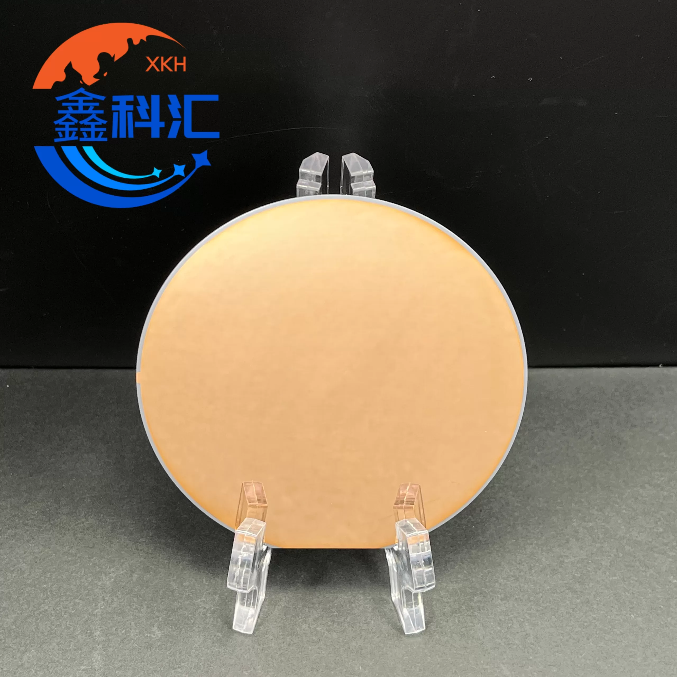
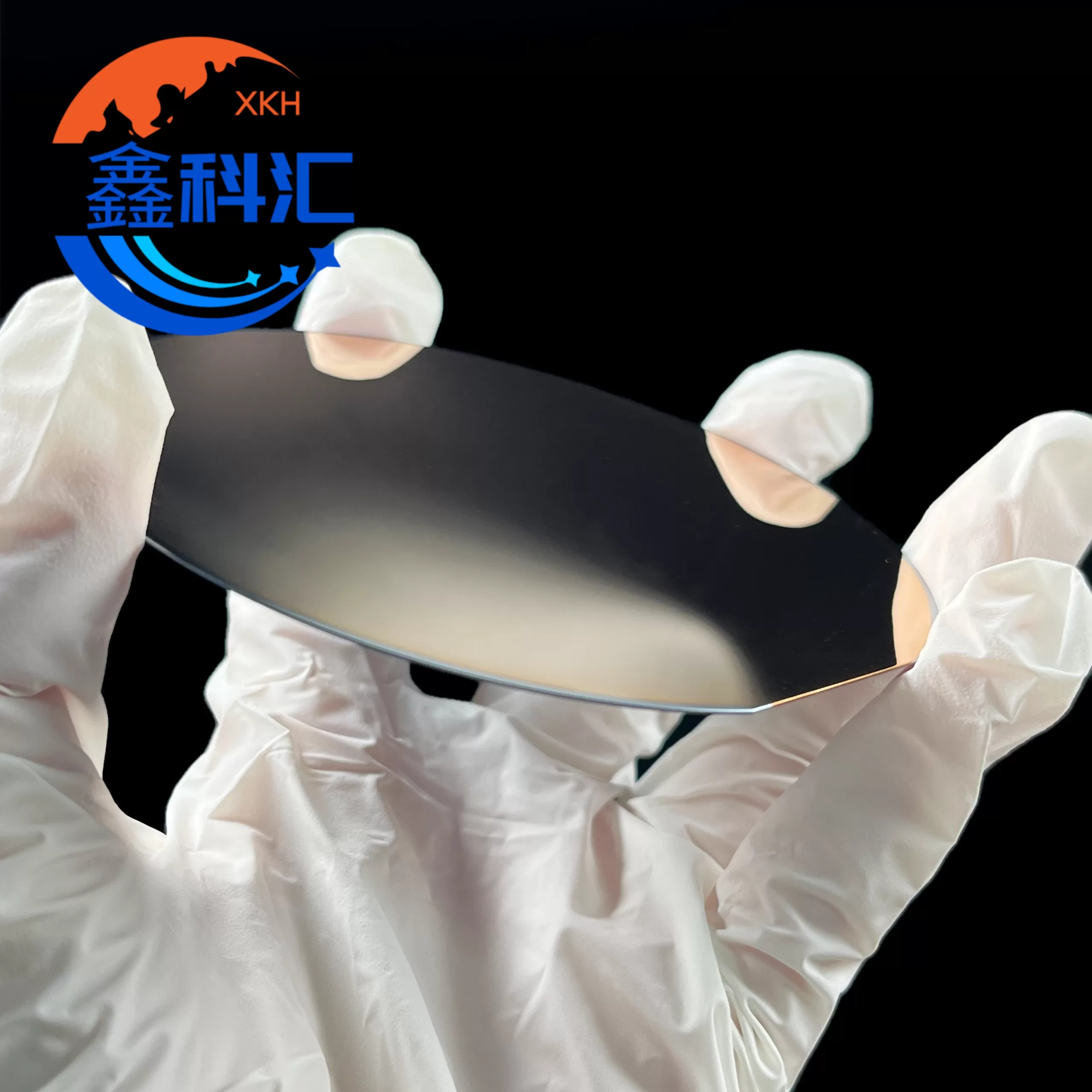
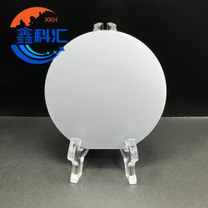
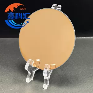
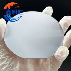
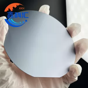
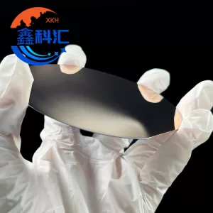
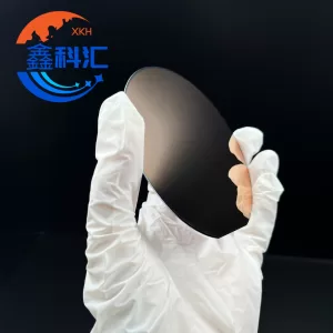
This 4-inch (100 mm) N-type, P-doped silicon wafer with <100> crystalline orientation is coated with a 100 nm Titanium (Ti) adhesion layer and a 200 nm Copper (Cu) conductive layer.
The Ti layer functions as a strong adhesion buffer and diffusion barrier, enhancing Cu film attachment and thermal stability. The Cu layer provides high electrical conductivity, making this wafer suitable for microelectronics, MEMS devices, sensors, and research applications.
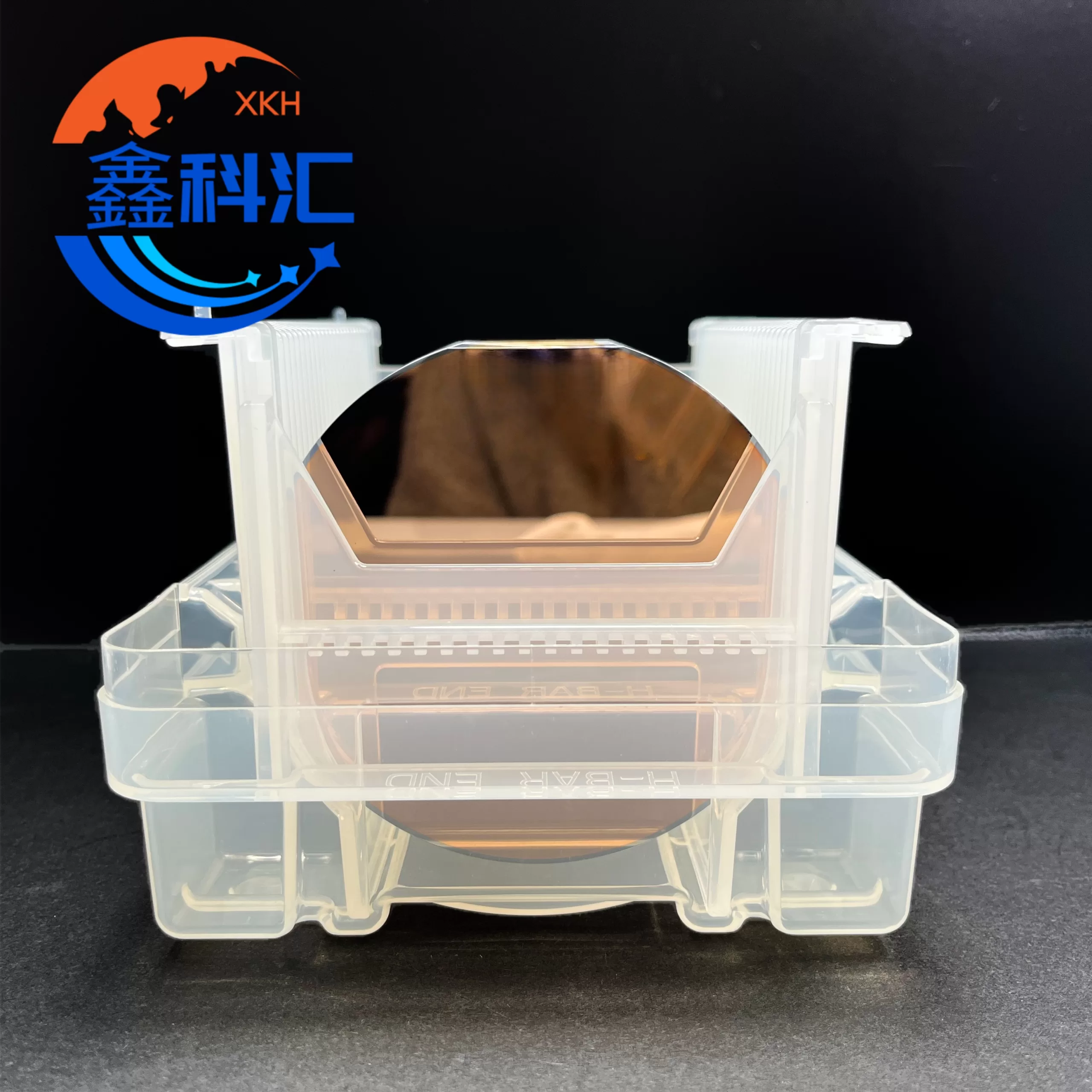
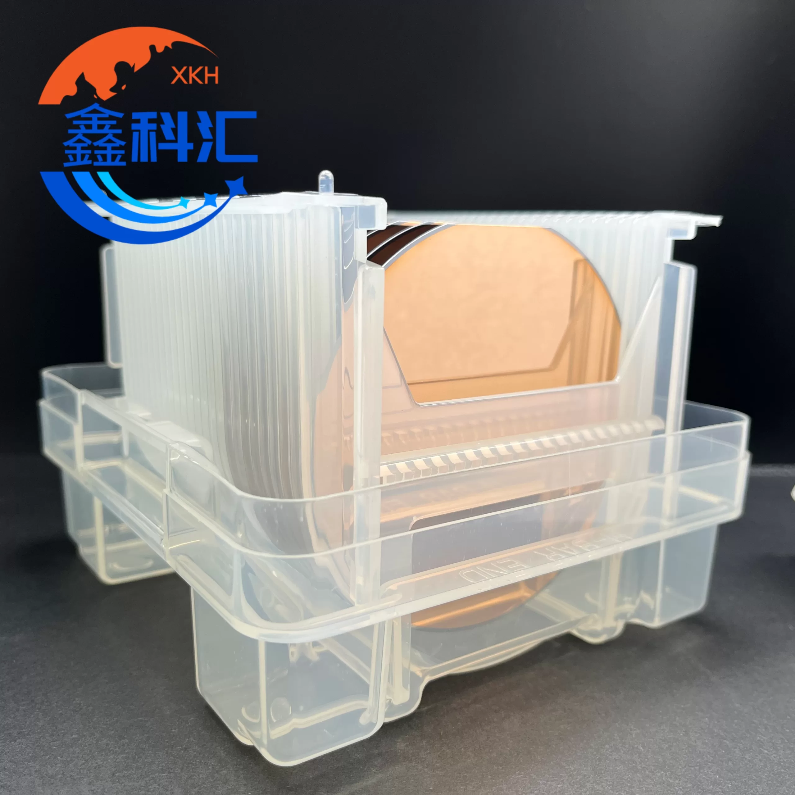
The wafer is single-side polished (SSP) and supplied in cleanroom packaging, ensuring contamination-free handling for precision applications. The thin-film structure is optimized for uniform thickness, consistent electrical performance, and reliable adhesion.
This wafer is ideal for applications that require a high-quality Cu/Ti interface on silicon substrates.
Tekniset tiedot
| Parametri | Tekniset tiedot |
|---|---|
| Kiekon koko | 4 inch diameter × 0.525 mm thickness |
| Kiekko Tyyppi | Prime Grade, N-type, P-doped |
| Crystalline Orientation | <100> |
| Kiillotus | Single Side Polished (SSP) |
| Ti Adhesion Layer Thickness | 100 nm |
| Cu Conductive Layer Thickness | 200 nm |
| Cu Film Structure | Polycrystalline, uniform deposition |
| Electrical Resistivity | 1–10 Ω·cm |
| Pinnan karheus | As-grown (typical, not specified) |
| Deposition Method | High-vacuum PVD (sputtering or e-beam) |
| Package | Single wafer in 100-class plastic bag inside 1000-class cleanroom |
Sovellukset
Semiconductor interconnect layers
MEMS microstructures and electrodes
Sensor devices and contact pads
Research and development in thin-film electronics
High-conductivity test wafers for microfabrication
Tärkeimmät ominaisuudet
Ti adhesion layer ensures strong Cu-Si bonding
200 nm Cu layer provides a low-resistance conductive path
Ti layer acts as a diffusion barrier to improve thermal stability
PVD deposition ensures consistent thickness and surface quality
Cleanroom packaging maintains wafer cleanliness and integrity
Usage and Storage Notes
Handle in a cleanroom or low-dust environment
Optimize temperature and processing conditions for high-temperature applications to prevent Cu/Si interdiffusion
Store in a dry, low-stress environment to maintain thin-film integrity
Avoid direct contact with the coated surface
FAQ
1. What is the uniformity of the Cu/Ti thin films on the wafer?
The Ti adhesion layer and Cu conductive layer are deposited using high-vacuum PVD techniques, ensuring uniform thickness across the 4-inch wafer. The Cu film thickness is 200 nm and the Ti layer is 100 nm, with minimal variation suitable for microelectronics and research applications.
2. Can this wafer be used in high-temperature processes?
Yes, but precautions are recommended. The Ti layer acts as a diffusion barrier to prevent Cu from diffusing into the silicon substrate. Optimizing temperature and processing conditions helps maintain film integrity and uniformity.
3. How should the wafer be stored and handled?
The wafer should be handled in a cleanroom or low-dust environment. Store in a dry, low-stress environment and avoid touching the coated surface directly. Each wafer is supplied in a 100-class plastic bag inside a 1000-class cleanroom package.
Arviot
Tuotearvioita ei vielä ole.