Focus on the field of new material !

Gallium Phosphide (GaP) wafers have emerged as critical materials in the realm of electronic and optoelectronic applications, owing to their unique combination of properties and versatile fabrication processes. This comprehensive review elucidates the properties, fabrication techniques, and diverse applications of GaP wafers, shedding light on their significance across various industries.
The paper commences with an overview of the fundamental properties of GaP wafers. GaP possesses a direct bandgap, making it highly suitable for optoelectronic devices such as light-emitting diodes (LEDs) and laser diodes. Its bandgap energy, approximately 2.26 eV, corresponds to green light emission, making it pivotal in various illumination applications. Additionally, GaP exhibits excellent optical transparency in the visible and near-infrared spectrum, facilitating efficient light transmission and emission. Moreover, GaP demonstrates good electrical conductivity and mechanical strength, along with moderate thermal conductivity, rendering it suitable for high-performance semiconductor devices.
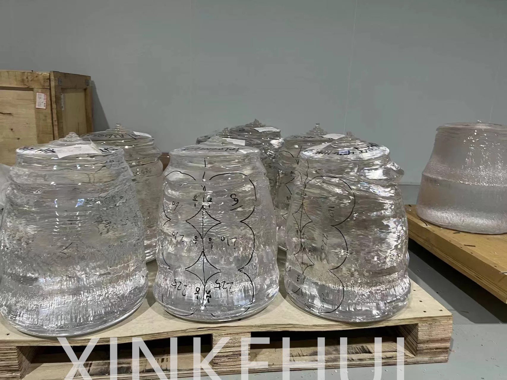
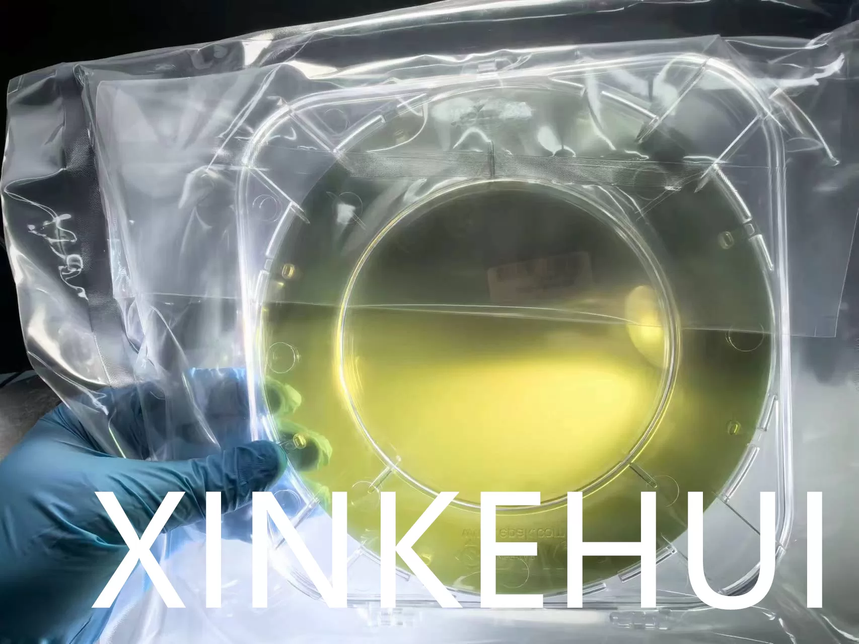
Subsequently, the fabrication techniques employed in the production of GaP wafers are explored. These include techniques such as Metalorganic Vapor Phase Epitaxy (MOVPE), Molecular Beam Epitaxy (MBE), and Liquid Phase Epitaxy (LPE). Each method offers distinct advantages in terms of crystal quality, scalability, and cost-effectiveness, catering to the diverse needs of the industry. Moreover, doping processes are discussed, elucidating how intentional introduction of impurities can tailor the electronic and optical properties of GaP wafers to meet specific application requirements.
The paper then delves into the wide-ranging applications of GaP wafers across different sectors. In the realm of optoelectronics, GaP wafers serve as the backbone for the production of LEDs, laser diodes, and photodetectors, enabling advancements in lighting technology, optical communication, and sensing applications. Moreover, GaP-based solar cells exhibit promising performance in space applications, owing to their high efficiency and radiation resistance. In the field of semiconductor devices, GaP wafers are utilized in high-frequency transistors, diodes, and power electronics, catering to the demands of modern electronics and telecommunications infrastructure.
Beyond traditional electronics, GaP wafers find applications in emerging technologies such as photonics, where they are employed in waveguides, modulators, and optical switches, paving the way for compact and efficient optical communication systems. Furthermore, GaP-based chemical sensors demonstrate sensitivity to specific chemical species, offering potential solutions for environmental monitoring and industrial safety. In biomedical applications, GaP wafers play a role in biosensors and imaging systems, facilitating advancements in healthcare diagnostics and research.
Additionally, GaP wafers find niche applications in quantum dots, military, and aerospace technologies. Quantum dots grown on GaP substrates exhibit unique quantum properties, holding promise for quantum computing, cryptography, and advanced display technologies. In military and aerospace sectors, GaP-based devices contribute to missile guidance systems, infrared sensors, and satellite communication, bolstering national security and exploration endeavors.
In conclusion, Gallium Phosphide (GaP) wafers stand as indispensable materials in the realm of electronic and optoelectronic technologies, underpinning advancements across a multitude of industries. Their unique properties, versatile fabrication techniques, and diverse applications underscore their significance in modern science and engineering. As research and innovation continue to drive technological progress, GaP wafers are poised to play an increasingly pivotal role in shaping the future of electronics, photonics, and beyond.

Gallium Phosphide (GaP) wafers, with their remarkable properties and versatile characteristics, find extensive applications across a wide array of industries and technological domains. This comprehensive exploration delves into the diverse applications of GaP wafers, highlighting their significance in modern science, engineering, and everyday life.
Optoelectronics: GaP wafers serve as fundamental building blocks in the realm of optoelectronic devices, facilitating advancements in lighting, communication, and sensing technologies. In particular, GaP-based light-emitting diodes (LEDs) are widely utilized in various lighting applications, including display backlighting, automotive lighting, and general illumination. The superior efficiency and color purity of GaP LEDs make them indispensable in achieving energy-efficient lighting solutions. Furthermore, GaP-based laser diodes enable precise and high-intensity light emission, finding applications in laser pointers, optical storage systems, and medical devices. Additionally, GaP photodetectors and photovoltaic cells contribute to optical sensing and solar energy harvesting applications, respectively, offering reliable performance in diverse environmental conditions.
Semiconductor Devices: GaP wafers play a pivotal role in the fabrication of semiconductor devices, catering to the demands of modern electronics and telecommunications infrastructure. High-frequency transistors based on GaP wafers exhibit exceptional performance in radio frequency (RF) amplification and wireless communication systems, enabling enhanced data transmission and signal processing capabilities. Moreover, GaP diodes find applications in rectification, signal modulation, and power conversion, contributing to the efficiency and reliability of electronic circuits in various consumer, industrial, and automotive electronics.
Photonics and Optical Communication: In the burgeoning field of photonics, GaP wafers enable the realization of compact and efficient optical components for communication and sensing applications. GaP waveguides, modulators, and optical switches offer precise control and manipulation of light signals, facilitating the development of high-speed data transmission systems, optical interconnects, and integrated photonic circuits. Moreover, GaP-based nonlinear optical devices exhibit nonlinear optical phenomena such as frequency conversion and optical parametric amplification, enabling the generation of coherent light sources across a broad spectral range.
Solar Cells and Renewable Energy: GaP-based solar cells hold promise for renewable energy applications, particularly in space and aerospace sectors where high efficiency and radiation resistance are paramount. GaP solar cells, integrated into multi-junction photovoltaic modules, demonstrate superior performance in converting solar energy into electrical power, making them ideal for space exploration missions, satellite power systems, and extraterrestrial habitats. Furthermore, ongoing research efforts focus on enhancing the efficiency and scalability of GaP solar cells for terrestrial applications, aiming to harness solar energy more effectively and sustainably on Earth.
Chemical and Biological Sensing: GaP-based sensors exhibit sensitivity to specific chemical and biological species, offering valuable solutions for environmental monitoring, industrial safety, and biomedical diagnostics. GaP sensors, integrated into gas detectors, environmental analyzers, and chemical sensors, enable real-time detection and quantification of hazardous substances, contributing to workplace safety and pollution control efforts. Moreover, GaP biosensors, functionalized with biorecognition elements, facilitate the rapid and selective detection of biomolecules, pathogens, and disease markers, empowering healthcare professionals with diagnostic tools for disease prevention and treatment.
Military and Aerospace Technologies: In the defense and aerospace sectors, GaP-based devices play critical roles in various applications, ranging from infrared imaging and sensing to secure communication and navigation systems. GaP-based infrared detectors and focal plane arrays provide enhanced thermal imaging capabilities for night vision, surveillance, and target acquisition purposes, enabling military personnel and law enforcement agencies to operate effectively in low-light conditions. Additionally, GaP-based optoelectronic components support secure communication networks, encrypted data transmission, and precision-guided munitions, bolstering national security and defense capabilities.
Emerging Technologies: Beyond traditional applications, GaP wafers contribute to emerging technologies such as quantum information science, nanotechnology, and biomedical engineering. GaP quantum dots, fabricated on GaP substrates, exhibit unique quantum properties and hold promise for quantum computing, quantum cryptography, and advanced display technologies. Moreover, GaP nanostructures, fabricated through innovative nanofabrication techniques, enable the development of novel nanoelectronic devices, sensors, and biomedical implants, opening new frontiers in materials science and nanotechnology.
In conclusion, Gallium Phosphide (GaP) wafers emerge as indispensable materials in the modern technological landscape, driving innovations across diverse industries and scientific disciplines. From optoelectronics and semiconductor devices to photonics, renewable energy, and beyond, GaP wafers continue to empower researchers, engineers, and innovators worldwide with their exceptional properties and versatile applications. As research and development efforts advance, GaP wafers are poised to play an increasingly pivotal role in shaping the future of technology, enabling breakthroughs that address global challenges and enhance quality of life for generations to come.
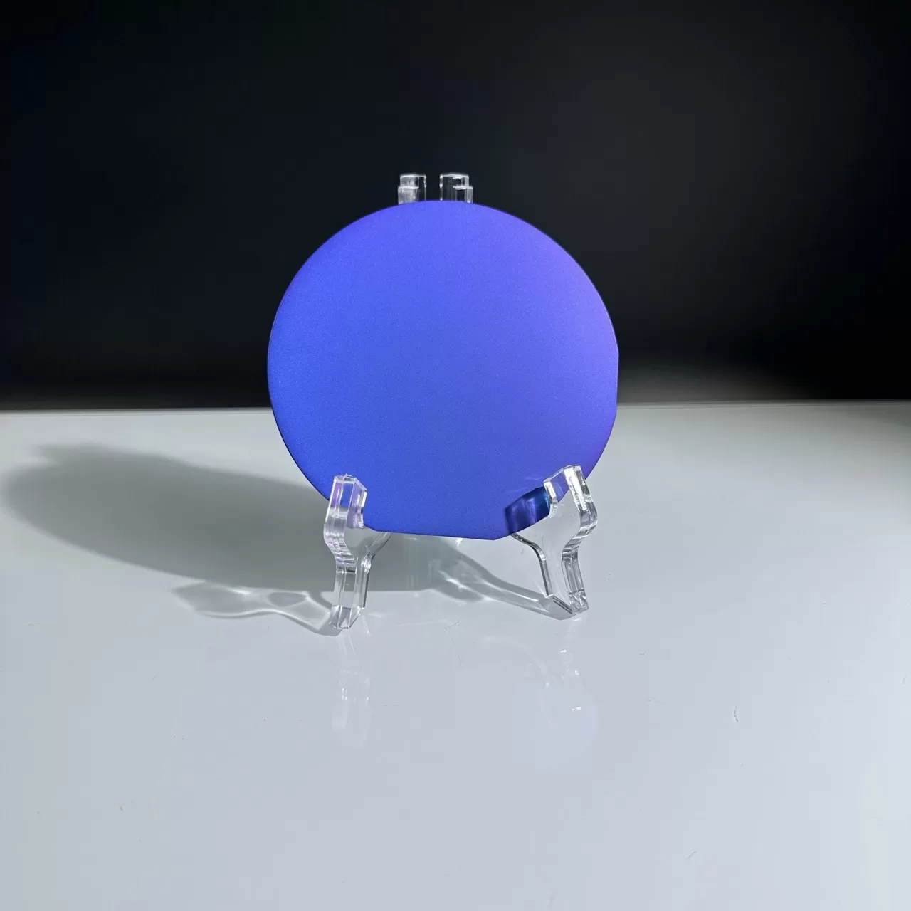
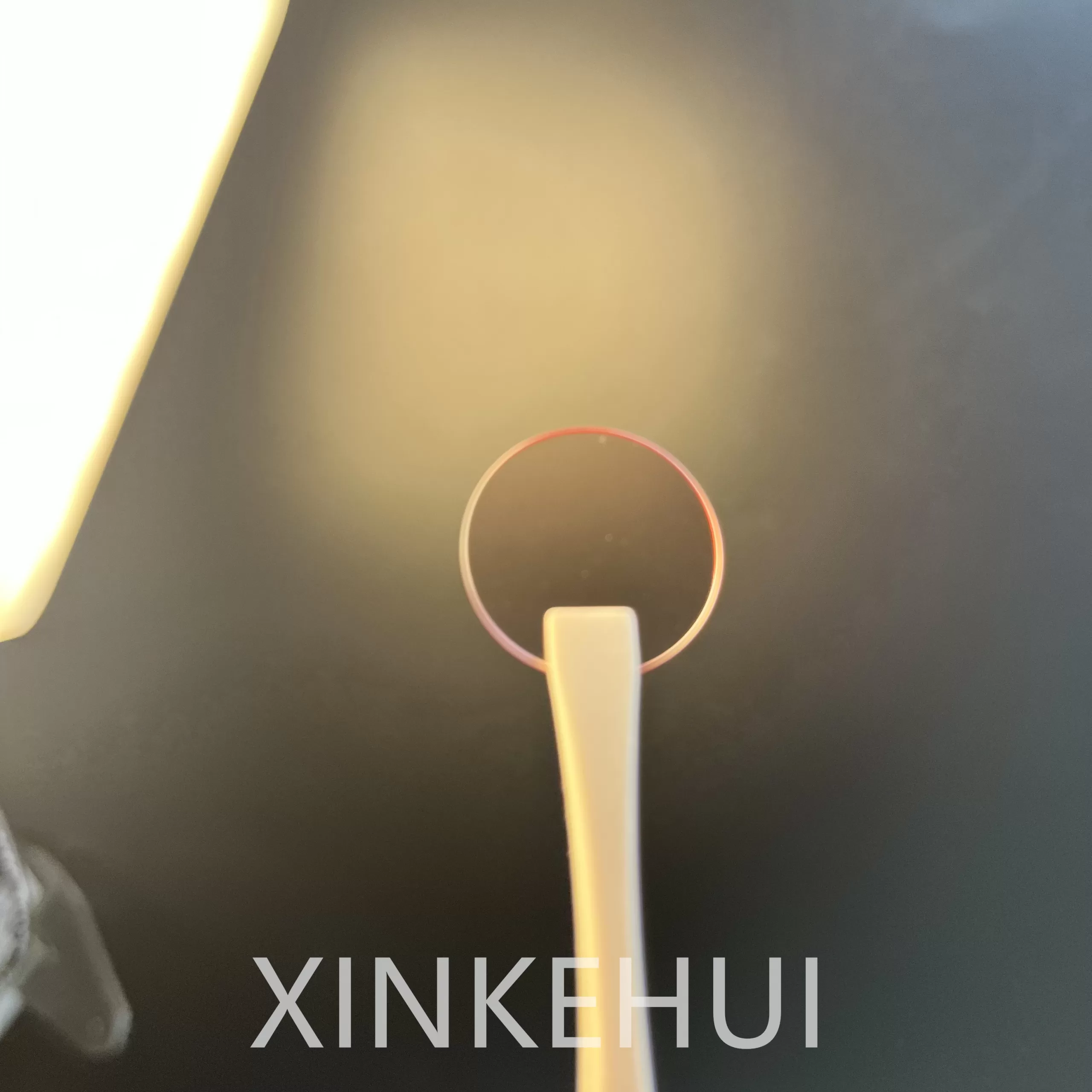
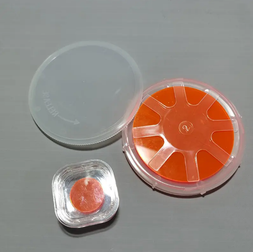
Below are just some of the available GaP substrates.
GaP Wafer undoped (100) 2″x 0.5 DSP
GaP Wafer, Undoped (111) 10x10x0.35 mm, DSP
GaP Wafer, Undoped (111) 10x10x0.5 mm, DSP
GaP Wafer, S doped (111) 2″x0.5 mm, DSP
GaP Wafer, undoped (100) 10x10x0.5 mm, SSP
GaP Wafer, undoped (100) 10x10x0.5 mm, DSP
GaP Wafer, undoped (100) 10x3x0.5 mm, SSP
GaP wafer undoped (100) 2″ diaX 0.45mm SSP, R: 1.5×10^14 ohm.cm, Semi-Insulating
GaP wafer, S doped, (100), 2″ dia x 0.5 mm, SSP
GaP wafer, S doped, (100), 2″ dia x 0.50 mm, DSP
GaP wafer, S doped, (100), 5 x 5 x 0.5 mm, SSP
GaP Wafer, undoped (110) 10x10x0.45 mm, SSP
GaP Wafer, undoped (110) 10x10x0.5 mm, DSP
GaP Wafer, undoped (110) 5x5x0.2 mm, DSP
Typical Physical Properties | ||
| Crystal Structure | Cubic. a =5.4505 A | |
| Growth Method | CZ (LEC) | |
| Density | 4.13 g/cm3 | |
| Melt Point | 1480 oC | |
| Thermal Expansion | 5.3 x10⁻⁶ / oC | |
| Dopant | S doped | undoped |
| Crystal growth axis | <111> or <100> | <100> or <111> |
| Conducting Type | N | N |
| Carrier Concentration | 2 ~ 8 x10¹⁷ /cm3 | 4 ~ 6 x10¹⁶ /cm3 |
| Resistivity | ~ 0.03 ohm-cm | ~ 0.3 ohm-cm |
| EPD | < 3×10⁵ | < 3×10⁵ |
Gallium Phosphide (GaP) wafers exhibit a diverse array of properties that render them invaluable in a wide range of electronic and optoelectronic applications. This comprehensive exploration delves into the intricate characteristics and functionalities of GaP wafers, elucidating their significance in modern science, engineering, and industry.
Optical Properties: GaP wafers boast exceptional optical properties, making them well-suited for optoelectronic devices and photonic applications. With a direct bandgap energy of approximately 2.26 electron volts (eV), GaP enables efficient light emission in the visible spectrum, particularly in the green wavelength range. This property is exploited in the fabrication of light-emitting diodes (LEDs) for various illumination and display applications. Moreover, GaP exhibits high optical transparency in the visible and near-infrared regions, allowing for the transmission and manipulation of light in optical components and communication systems.
Electrical Properties: In addition to their optical prowess, GaP wafers demonstrate favorable electrical characteristics essential for semiconductor devices and electronic circuits. GaP possesses intrinsic semiconductor behavior, with a bandgap that determines its electrical conductivity properties. By introducing dopant atoms such as silicon or zinc into the GaP crystal lattice, the conductivity and carrier concentration can be controlled, enabling the fabrication of diodes, transistors, and other semiconductor devices. Furthermore, GaP exhibits high electron mobility, facilitating fast charge transport and high-frequency operation in RF (radio frequency) devices.
Thermal Properties: GaP wafers exhibit moderate thermal conductivity, making them suitable for applications requiring efficient heat dissipation and thermal management. The thermal conductivity of GaP, typically in the range of 100-200 W/m·K, allows for the effective removal of heat generated during device operation, thereby enhancing reliability and performance. This property is particularly important in high-power semiconductor devices, where excessive heat can degrade device performance and lead to reliability issues.
Mechanical Properties: Mechanically, GaP wafers display robustness and durability, enabling ease of handling during processing and assembly. GaP crystals exhibit a high degree of crystalline perfection, with low defect densities and minimal crystallographic imperfections. This results in wafers with smooth surfaces and uniform thickness, essential for the fabrication of high-quality electronic and optoelectronic devices. Moreover, GaP wafers demonstrate resilience to mechanical stress and deformation, ensuring long-term stability and reliability in various operating conditions.
Chemical Stability: GaP is chemically stable under normal operating conditions, exhibiting resistance to oxidation, corrosion, and chemical degradation. This inherent stability is advantageous for device reliability and longevity, particularly in harsh environments or demanding applications where exposure to moisture, contaminants, or corrosive agents is prevalent. GaP wafers maintain their structural integrity and electrical properties over extended periods, ensuring consistent performance and minimal degradation over time.
Wide Bandgap Engineering: One of the most notable properties of GaP is its ability to be tailored through wide bandgap engineering techniques. By selectively doping the GaP crystal with specific impurities, the bandgap energy and electronic properties can be precisely controlled to suit the requirements of different device applications. This flexibility enables the design and optimization of GaP-based devices for specific wavelengths, operating voltages, and performance metrics, expanding the range of potential applications across various industries.
Radiation Hardness: GaP wafers exhibit radiation hardness, making them suitable for use in radiation-rich environments such as space and nuclear applications. Unlike some other semiconductor materials that degrade under ionizing radiation, GaP maintains its electrical and optical properties even when exposed to high levels of radiation. This property is particularly advantageous for space-based electronics, where reliability and resilience to cosmic radiation are critical for mission success.
In conclusion, Gallium Phosphide (GaP) wafers possess a rich tapestry of properties that underpin their versatility and utility in electronic and optoelectronic applications. From their optical brilliance and electrical conductivity to their thermal resilience and chemical stability, GaP wafers embody a harmonious blend of characteristics essential for modern technology. As research and development efforts continue to advance, GaP wafers are poised to play an increasingly pivotal role in shaping the future of electronics, photonics, and beyond, driving innovation and enabling breakthroughs that address global challenges and enhance quality of life.
Gallium Phosphide (GaP) wafers offer a multitude of advantages across various applications, stemming from their unique combination of properties and versatile characteristics. This comprehensive exploration elucidates the numerous advantages of GaP wafers, highlighting their significance in modern science, engineering, and industry.
1. Optoelectronic Efficiency: GaP wafers exhibit high optical efficiency, making them ideal for optoelectronic devices such as light-emitting diodes (LEDs) and laser diodes. The direct bandgap nature of GaP enables efficient light emission, resulting in bright and uniform illumination with minimal energy consumption. This property is particularly advantageous in applications where energy efficiency and long-term reliability are paramount.
2. Wide Bandgap Engineering: GaP wafers offer versatility in bandgap engineering, allowing for precise control over the optical and electronic properties of semiconductor devices. Through intentional doping and alloying techniques, the bandgap of GaP can be tailored to match specific application requirements, enabling the development of custom-designed optoelectronic components with optimized performance and functionality.
3. Optical Transparency: GaP wafers exhibit excellent optical transparency across the visible and near-infrared spectrum, enabling efficient transmission and detection of light signals. This property is advantageous in applications such as photodetectors, optical sensors, and photovoltaic cells, where high optical sensitivity and signal fidelity are essential for accurate measurement and detection.
4. Mechanical Robustness: GaP wafers possess inherent mechanical strength and durability, ensuring reliable performance in harsh operating environments. This mechanical robustness makes GaP wafers suitable for integration into ruggedized devices and systems used in aerospace, automotive, and industrial applications, where resistance to mechanical stress, vibration, and thermal cycling is critical.
5. Chemical Stability: GaP wafers exhibit excellent chemical stability, rendering them resistant to degradation and corrosion in diverse chemical environments. This property is advantageous in applications such as chemical sensors, environmental monitoring, and biomedical devices, where sensor longevity and stability are essential for accurate and reliable operation over extended periods.
6. High Breakdown Voltage: GaP wafers demonstrate a relatively high breakdown voltage, allowing for the fabrication of power semiconductor devices with enhanced voltage-handling capabilities. This property is advantageous in power electronics applications, where GaP-based devices such as diodes and transistors can withstand high voltage levels without experiencing electrical breakdown or failure, ensuring robust performance in high-power circuits and systems.
7. Thermal Conductivity: While not as high as some other semiconductor materials, GaP wafers exhibit moderate thermal conductivity, aiding in the efficient dissipation of heat generated during device operation. This property is advantageous in high-power electronic devices and optoelectronic components, where thermal management is crucial for maintaining device performance and reliability under elevated operating temperatures.
8. Compatibility with Fabrication Techniques: GaP wafers are compatible with a variety of fabrication techniques, including epitaxial growth methods such as Metalorganic Vapor Phase Epitaxy (MOVPE) and Molecular Beam Epitaxy (MBE), as well as conventional semiconductor processing techniques such as lithography, etching, and metallization. This compatibility allows for the integration of GaP wafers into existing semiconductor manufacturing processes, facilitating the production of complex and highly integrated devices with minimal process modifications.
9. Radiation Resistance: GaP-based devices exhibit inherent radiation resistance, making them suitable for applications in radiation-rich environments such as space, aerospace, and nuclear industries. This property is advantageous in space exploration missions, satellite communication systems, and nuclear power plants, where GaP-based devices can operate reliably and maintain performance integrity in the presence of ionizing radiation.
10. Emerging Applications: GaP wafers hold promise for emerging applications in quantum information science, nanotechnology, and biomedical engineering. As researchers explore the unique quantum properties and nanoscale phenomena exhibited by GaP-based materials, new opportunities emerge for the development of next-generation devices and technologies with enhanced functionality and performance.
In conclusion, Gallium Phosphide (GaP) wafers offer a myriad of advantages that position them as indispensable materials in the modern technological landscape. From their high optical efficiency and versatile bandgap engineering capabilities to their mechanical robustness, chemical stability, and compatibility with fabrication techniques, GaP wafers empower researchers, engineers, and innovators to push the boundaries of science and engineering, driving advancements across diverse industries and applications. As research and development efforts continue to evolve, GaP wafers are poised to play an increasingly pivotal role in shaping the future of technology, enabling transformative breakthroughs that address global challenges and improve quality of life for generations to come.