
Glass wafers are increasingly used in advanced semiconductor packaging as carrier wafers, interposers, through-glass-via substrates, MEMS packaging substrates and temporary bonding platforms. Their dimensional stability, electrical insulation, optical transparency and adjustable coefficient of thermal expansion make them suitable for fan-out packaging, 2.5D and 3D integration, RF modules and heterogeneous integration.
However, the performance of a glass wafer is not determined only by its surface flatness, thickness or through-glass-via accuracy. The quality of the wafer edge is equally important.
Small edge chips, subsurface cracks or poorly processed bevels can significantly reduce the mechanical strength of a glass wafer. These defects may cause wafer breakage during automated handling, thermal processing, bonding, grinding or debonding. For this reason, glass wafer edge quality must be carefully specified and inspected for advanced packaging applications.
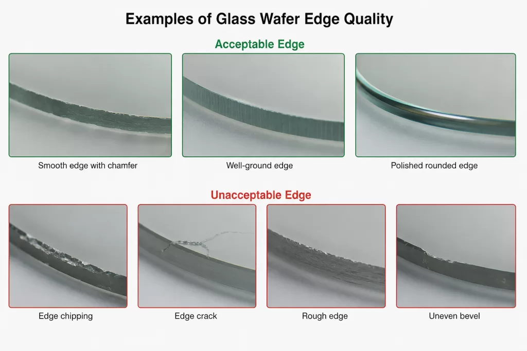
Why Glass Wafer Edge Quality Matters
Glass is a brittle material. Unlike metals, it has limited ability to deform plastically when exposed to mechanical stress. Once a crack forms at the edge, stress can concentrate around the crack tip and cause the defect to propagate through the wafer.
The theoretical strength of defect-free glass can be extremely high, but practical glass strength is usually controlled by surface and edge flaws introduced during cutting, grinding, transportation and handling. Corning notes that glass strength is strongly affected by defects and that damage control is essential for maintaining mechanical reliability.
In an advanced packaging line, glass wafers may experience:
- Robotic wafer handling
- Vacuum chucking
- Spin coating
- Lithography
- Metal deposition
- Temporary bonding
- Thermal cycling
- Back grinding
- Chemical cleaning
- Laser processing
- Wafer-level molding
- Mechanical or laser debonding
An edge defect that appears harmless during incoming inspection may grow after repeated mechanical and thermal loading.
Good edge quality therefore helps improve:
- Wafer breakage resistance
- Process yield
- Equipment uptime
- Handling stability
- Bonding reliability
- Thermal-cycle durability
- Overall manufacturing consistency
Main Types of Glass Wafer Edge Defects
1. Edge Chipping
Edge chipping refers to small pieces of glass breaking away from the wafer perimeter. It is one of the most common defects produced during wafer cutting, contouring or edge grinding.
Chips may vary in:
- Radial depth
- Tangential length
- Vertical height
- Distance from the wafer surface
- Crack extension beneath the visible chip
Large chips can interfere with edge-grip handling systems or create local stress concentrations. Even relatively small chips may contain hidden cracks extending beyond the visible damaged area.
For advanced packaging applications, the chip acceptance limit should be defined using measurable dimensions rather than descriptions such as “small chip” or “minor damage.”
2. Microcracks and Subsurface Damage
Microcracks are often more dangerous than visible edge chips because they may not be easily detected with normal visual inspection.
They can be produced by:
- Mechanical sawing
- Coarse grinding
- Improper tool feed rate
- Excessive contact pressure
- Worn diamond tools
- Impact during transportation
- Wafer-to-wafer contact
- Improper cassette loading
Subsurface damage may remain underneath an apparently smooth edge. During heating, bonding or grinding, the crack can propagate and cause sudden wafer fracture.
3. Rough or Irregular Edge Surfaces
A rough edge contains grooves, pits, tool marks and irregularities created during cutting or grinding. These surface features can act as crack initiation sites.
The required edge finish depends on:
- Glass composition
- Wafer thickness
- Wafer diameter
- Subsequent thermal processes
- Mechanical handling method
- Temporary bonding conditions
- Required breakage resistance
For high-reliability processes, the edge normally requires controlled fine grinding or polishing after wafer contouring.
4. Bevel and Chamfer Defects
A bevel or chamfer is commonly applied to the top and bottom perimeter of a wafer. Its purpose is to remove sharp corners, reduce edge stress and improve handling resistance.
Common bevel-related defects include:
- Uneven bevel width
- Excessive bevel angle
- Incomplete beveling
- Sharp residual corners
- Bevel asymmetry
- Local over-grinding
- Surface chips along the bevel transition
The bevel geometry must be uniform around the full wafer circumference.
5. Edge Contamination
Particles, grinding residues, organic contamination and metallic debris may remain on the glass edge after machining.
Edge contamination can be transferred to:
- Wafer surfaces
- Bonding interfaces
- Coating equipment
- Vacuum chucks
- Process chambers
- Transport cassettes
For semiconductor packaging applications, cleaning must include the wafer perimeter and bevel area, not only the front and back surfaces.
Important Glass Wafer Edge Quality Parameters
There is no single universal edge specification suitable for every advanced packaging project. Requirements should be established according to the glass material, wafer geometry and downstream process.
The following parameters are commonly considered.
Maximum Allowable Edge Chip Size
Edge chips are usually controlled by specifying maximum dimensions.
Typical inspection parameters include:
- Maximum radial chip depth
- Maximum tangential chip length
- Maximum chip height
- Maximum number of chips per wafer
- Minimum spacing between chips
- Whether cracks extending from the chip are permitted
A specification may also divide chips into different zones, such as the bevel area, edge exclusion zone and active wafer area.
The appropriate limit depends heavily on wafer thickness and process risk. A chip size acceptable for a thick carrier wafer may be unacceptable for an ultra-thin interposer substrate.
Crack Acceptance Criteria
For high-reliability packaging applications, visible cracks extending from the edge are normally unacceptable.
The specification should clarify whether it prohibits:
- Radial cracks
- Circumferential cracks
- Corner cracks
- Bevel cracks
- Subsurface cracks
- Cracks detectable only under polarized light or enhanced illumination
Because crack detection capability depends on the inspection method, the inspection equipment and magnification should also be stated.
Edge Roughness
Edge roughness influences mechanical strength and crack initiation risk.
Edge roughness may be evaluated using:
- Optical profilometry
- Contact profilometry
- Confocal microscopy
- Microscopic surface comparison
- Process-controlled grinding specifications
In many production environments, suppliers control edge quality through qualified machining parameters rather than measuring roughness on every wafer.
For critical projects, however, an agreed edge roughness limit may be included in the technical specification.
Bevel Width and Bevel Angle
The bevel should be wide enough to remove sharp corners but not so large that it reduces the usable wafer area or creates handling problems.
Important bevel parameters include:
- Upper bevel width
- Lower bevel width
- Bevel angle
- Edge crown radius
- Symmetry between both sides
- Circumferential uniformity
The correct bevel design depends on wafer thickness, equipment compatibility and whether the wafer will be temporarily bonded to another substrate.
Edge Profile and Roundness
The wafer perimeter must maintain the required diameter, roundness and edge profile.
Important geometrical parameters include:
- Wafer diameter tolerance
- Circularity
- Local edge deviation
- Notch geometry
- Flat geometry, where applicable
- Notch or flat position accuracy
Poor circularity may cause alignment errors, unstable rotation or problems with edge-gripping systems.
Edge Exclusion Zone
The edge exclusion zone defines the region near the wafer perimeter where surface defects, coating nonuniformity or pattern loss may be accepted.
This parameter is especially important for:
- Redistribution layer processing
- Lithography
- Metal plating
- Wafer-level bonding
- Through-glass-via metallization
- Thin-film deposition
The edge exclusion zone should be coordinated with the bevel geometry. If it is too narrow, the active pattern may extend into a mechanically unstable region.
Factors That Determine the Required Edge Quality
Glass Composition
Different glass materials have different hardness, thermal expansion, chemical durability and fracture behavior.
Common materials include:
- Borosilicate glass
- Aluminosilicate glass
- Fused silica
- Quartz glass
- Alkali-free glass
- Photosensitive glass
- Specialty glass ceramics
SCHOTT notes that contact with materials of similar or greater hardness can introduce indentations and cracks into glass surfaces. This illustrates why machining tools, handling materials and contact conditions must be carefully controlled.
Wafer Thickness
Thin glass wafers are generally more sensitive to bending, local edge loading and handling damage.
As wafer thickness decreases:
- Edge strength becomes more critical
- Handling fixtures require better support
- Chip-size limits may need to be tightened
- Temporary bonding may become necessary
- Packaging and transportation requirements increase
Ultra-thin glass wafers may need to remain bonded to a carrier throughout several processing steps.
Wafer Diameter
Larger-diameter wafers experience greater bending moments during handling. A defect acceptable on a small research wafer may present a higher fracture risk on a 200 mm or 300 mm wafer.
Large wafers generally require:
- Better edge uniformity
- More controlled bevel geometry
- Lower defect density
- Improved cassette compatibility
- Automated full-circumference inspection
Thermal Processing Conditions
Advanced packaging often includes repeated heating and cooling steps. Differences in thermal expansion between glass, metals, polymers and temporary bonding adhesives can generate stress.
Glass carriers are frequently selected for their available thermal expansion ranges, high geometrical accuracy and suitability for fan-out and 3D packaging processes.
However, poor edge quality can undermine these benefits by providing sites where thermal stress initiates fracture.
Temporary Bonding and Debonding
Glass carrier wafers are commonly used to support thin silicon wafers or reconstructed wafers during temporary bonding processes.
Corning identifies surface quality, thickness control and edge strength as important properties of advanced packaging glass carriers.
During debonding, the glass edge may experience:
- Local peeling forces
- Vacuum loading
- Mechanical contact
- Thermal gradients
- Laser-induced stress
The edge specification should therefore be matched to the selected bonding and debonding method.
Through-Glass-Via Processing
Glass interposers and glass-core substrates may include thousands or millions of through-glass vias.
TGV glass supports compact packaging, high-density electrical interconnects and RF applications.
Although vias are usually located away from the wafer edge, the combined effects of via formation, metallization, thermal cycling and wafer handling can increase overall mechanical stress. Strong, defect-controlled edges are therefore important for TGV substrates.
Recommended Edge Processing Methods
Precision Mechanical Contouring
Mechanical contouring uses diamond tools to create the required wafer diameter, notch and edge profile.
Process quality depends on:
- Tool grit size
- Tool wear
- Spindle stability
- Feed speed
- Cooling
- Glass thickness
- Glass composition
- Machine vibration
A multi-step process using coarse shaping followed by fine grinding normally produces better strength than a single aggressive grinding step.
Edge Grinding
Edge grinding removes cutting damage and generates the final bevel or rounded profile.
A controlled process should minimize:
- Deep grinding grooves
- Thermal damage
- Large chips
- Residual cracks
- Bevel asymmetry
Grinding tools must be regularly inspected and replaced before wear begins to increase defect rates.
Edge Polishing
Edge polishing can further reduce surface roughness and remove residual grinding damage.
It may be used when:
- The wafer will experience high thermal stress
- Extremely low breakage rates are required
- The wafer is thin or large
- Optical edge quality is needed
- The wafer will undergo repeated handling cycles
Edge polishing adds cost, so it is not necessary for every project. Its value should be evaluated against the mechanical reliability requirements.
Laser Cutting or Laser Contouring
Laser-based processes may reduce direct mechanical contact, but they can introduce other defects, such as:
- Heat-affected zones
- Recast material
- Microcracks
- Residual stress
- Irregular edge morphology
Laser-cut edges may require additional finishing, depending on the glass type and laser process.
The choice between mechanical and laser processing should be based on total edge integrity rather than cutting speed alone.
Glass Wafer Edge Inspection Methods
Visual Inspection
Visual inspection is useful for identifying:
- Large chips
- Cracks
- Contamination
- Irregular bevels
- Notch damage
However, inspection conditions must be standardized.
The inspection specification should define:
- Lighting method
- Background
- Magnification
- Inspection angle
- Rotation speed
- Operator acceptance criteria
Optical Microscopy
Microscopy provides more accurate measurement of chip dimensions, crack length and bevel damage.
It is commonly used for:
- First article inspection
- Failure analysis
- Process qualification
- Customer acceptance inspection
- Defect classification
Automated Edge Inspection
Automated systems can scan the full wafer circumference and classify defects according to size and location.
Advantages include:
- Consistent inspection
- Reduced operator subjectivity
- Complete circumference coverage
- Digital defect records
- Statistical process monitoring
- Traceability by wafer
Automated inspection is particularly valuable for high-volume 200 mm and 300 mm production.
Polarized-Light Inspection
Polarized-light methods can help reveal residual stress patterns and some crack-related features in transparent glass.
This method may be useful after:
- Laser processing
- Thermal processing
- Bonding
- Aggressive grinding
- Localized mechanical damage
Mechanical Strength Testing
For process qualification, suppliers may perform sample-based strength testing rather than destructive testing of every production wafer.
Possible tests include:
- Ring-on-ring testing
- Four-point bending
- Three-point bending
- Edge strength testing
- Proof testing
- Thermal-cycle testing
Test results depend strongly on specimen geometry, loading configuration and surface condition. Therefore, strength values from different test methods should not be compared directly without considering the test procedure.
Example Glass Wafer Edge Specification Checklist
A technical drawing or purchase specification should clearly state the following:
| Parameter | Information to Specify |
|---|---|
| Glass material | Borosilicate, fused silica, aluminosilicate or other glass |
| Wafer diameter | Nominal diameter and tolerance |
| Wafer thickness | Nominal thickness and tolerance |
| Edge shape | Rounded, chamfered, beveled or custom profile |
| Bevel width | Upper and lower bevel dimensions |
| Bevel angle | Required nominal value and tolerance |
| Edge chip limit | Maximum radial depth, length and quantity |
| Crack requirement | No visible cracks or defined acceptance level |
| Edge roughness | Maximum Ra or qualified process level |
| Notch or flat | Geometry, size and orientation |
| Edge exclusion | Required exclusion width |
| Inspection method | Visual, microscopic or automated |
| Magnification | Minimum inspection magnification |
| Cleaning level | Particle and residue requirements |
| Packaging | Individual separation and edge protection |
| Strength testing | Test method and sampling frequency, if required |
Common Mistakes When Specifying Glass Wafer Edges
Using Vague Defect Descriptions
Terms such as “good edge,” “minor chipping” or “semiconductor quality” are not measurable.
A better specification defines chip dimensions, crack acceptance, inspection magnification and bevel geometry.
Copying Silicon Wafer Specifications Directly
Glass and silicon have different machining behavior and fracture characteristics.
A silicon wafer edge specification should not automatically be applied to glass without reviewing:
- Material properties
- Thickness
- Packaging process
- Handling equipment
- Thermal conditions
Ignoring Subsurface Damage
An edge may appear visually smooth while still containing subsurface cracks.
For high-risk applications, edge process qualification and sample-based strength testing may be necessary.
Specifying an Unnecessarily Perfect Edge
Extremely tight edge tolerances increase processing cost and inspection time.
The specification should reflect actual process risks rather than requesting the tightest possible value for every parameter.
Failing to Define Inspection Conditions
Two inspectors may report different results when lighting, magnification and chip-measurement methods are not standardized.
Inspection conditions should be agreed upon before mass production.
How Edge Quality Influences Advanced Packaging Yield
Edge defects can affect yield at multiple stages.
During Incoming Handling
Damaged edges may cause breakage when wafers are removed from shipping cassettes or loaded into automated equipment.
During Temporary Bonding
Uneven or chipped edges can affect adhesive flow, edge sealing and bond uniformity.
During Grinding and Thinning
Grinding places mechanical stress on the wafer and carrier system. Existing cracks can propagate rapidly under these conditions.
During Thermal Cycling
Repeated temperature changes can increase stress around chips, cracks and bevel irregularities.
During Debonding
Mechanical, thermal or laser debonding may expose the glass edge to concentrated forces.
During Final Singulation
For glass interposers or glass-core packages, weak wafer edges can contribute to unstable panel or wafer handling before final singulation.
Better edge control therefore reduces not only wafer breakage but also equipment contamination, production interruptions and downstream defect risk.
Choosing a Glass Wafer Supplier
When evaluating a glass wafer supplier for advanced packaging, buyers should ask:
- Which glass materials can be processed?
- What wafer diameters and thicknesses are available?
- Which edge profiles can be manufactured?
- How are edge chips measured?
- Are cracks completely prohibited?
- Is edge polishing available?
- Which inspection equipment is used?
- Can full-circumference inspection be provided?
- Is edge-strength testing available?
- How are thin wafers packaged and transported?
- Can inspection reports and defect images be supplied?
- Can the supplier process wafers with TGVs, cavities, notches or custom contours?
The supplier should also understand how the glass wafer will be used. A temporary bonding carrier, TGV interposer and MEMS cap wafer may require very different edge specifications.
Conclusion
Glass wafer edge quality is a critical but sometimes underestimated requirement in advanced semiconductor packaging.
Edge chips, microcracks, grinding damage and irregular bevels can reduce wafer strength and cause breakage during handling, bonding, thinning, thermal cycling or debonding. As wafer diameters increase and glass substrates become thinner, edge integrity becomes even more important.
A reliable specification should define measurable limits for chip size, cracks, bevel geometry, edge roughness, roundness and inspection conditions. At the same time, requirements should be matched to the actual packaging process to avoid unnecessary manufacturing cost.
By combining appropriate glass selection, controlled edge machining, effective cleaning and standardized inspection, manufacturers can improve glass wafer reliability and achieve more stable advanced packaging yields.
Frequently Asked Questions
What is the most important glass wafer edge defect?
Cracks are generally the most critical because they can propagate under mechanical or thermal stress. A small visible chip may also be dangerous when it contains an extended subsurface crack.
Are edge chips allowed on semiconductor glass wafers?
Small chips may be accepted in some applications, but their maximum size, quantity and location should be clearly specified. High-reliability or ultra-thin wafer applications normally require tighter limits.
Does every glass wafer need edge polishing?
No. Fine edge grinding may be sufficient for many carrier and research applications. Edge polishing is more valuable for thin wafers, large-diameter wafers, high-stress processes and applications requiring very low breakage rates.
Why is the glass wafer bevel important?
The bevel removes sharp corners, reduces stress concentration and improves resistance to handling damage. Poor bevel uniformity can create weak points around the wafer circumference.
Can normal visual inspection detect all edge cracks?
No. Small cracks and subsurface damage may require optical microscopy, automated edge inspection, polarized-light inspection or process qualification testing.
Should glass wafer edge requirements be the same as silicon wafer requirements?
Not necessarily. Glass and silicon differ in fracture behavior, processing methods and application conditions. Edge specifications should be developed specifically for the selected glass material and packaging process.