
High Purity Silicon Wafer’s abstract
High purity silicon wafers stand as fundamental building blocks in the realm of modern technology, serving as substrates for a diverse array of electronic and optoelectronic devices. This abstract delves into the intricacies of high purity silicon wafers, exploring their properties, fabrication processes, and applications across various industries. From semiconductor manufacturing to renewable energy and beyond, the significance of high purity silicon wafers in driving technological innovation cannot be overstated.
At the heart of high purity silicon wafers lies their exceptional material properties, which form the cornerstone of their utility in electronic devices. These wafers are meticulously engineered to exhibit high crystalline quality, low defect density, and precise thickness, enabling the creation of intricate semiconductor structures with unparalleled performance characteristics. The fabrication process involves multiple steps, including crystal growth, wafer slicing, surface preparation, and doping, each crucial for achieving the desired electronic properties.
In the realm of semiconductor manufacturing, high purity silicon wafers reign supreme as the foundation for integrated circuits (ICs), microprocessors, and memory chips. These wafers provide the platform upon which complex electronic circuits are etched, enabling the miniaturization and integration of countless electronic components into silicon chips. The relentless pursuit of smaller feature sizes and higher transistor densities drives ongoing advancements in silicon wafer technology, pushing the boundaries of Moore’s Law and fueling the digital revolution.
Beyond semiconductor manufacturing, high purity silicon wafers find applications in the burgeoning field of photovoltaics, where they play a pivotal role in solar cell fabrication. As the demand for renewable energy sources grows, silicon wafers serve as the bedrock for efficient and cost-effective solar panels, harnessing the power of sunlight to generate clean electricity. The relentless optimization of silicon wafer manufacturing processes and cell architectures has led to significant increases in solar cell efficiency, making solar energy an increasingly viable alternative to traditional fossil fuels.
In addition to their role in energy generation, high purity silicon wafers are integral to a myriad of other technological applications. In the realm of optoelectronics, these wafers enable the production of light-emitting diodes (LEDs), photodiodes, and optical sensors, facilitating advancements in lighting, telecommunications, and sensing technologies. Furthermore, high purity silicon wafers serve as the foundation for micro-electro-mechanical systems (MEMS), quantum computing devices, and biomedical sensors, underscoring their versatility and adaptability across diverse fields.
The continued evolution of high purity silicon wafer technology hinges on ongoing research and development efforts aimed at enhancing material quality, manufacturing processes, and device performance. From innovative crystal growth techniques to novel wafer slicing methods and advanced doping technologies, researchers are constantly pushing the boundaries of what is achievable with silicon wafers. Furthermore, the integration of silicon wafers with emerging materials such as graphene, carbon nanotubes, and perovskites holds promise for unlocking new frontiers in electronics, photonics, and beyond.
In conclusion, high purity silicon wafers represent a linchpin of modern technology, underpinning advancements in electronics, energy, and beyond. Their exceptional material properties, coupled with relentless innovation in fabrication techniques, make them indispensable components in a wide range of applications. As we continue to harness the potential of high purity silicon wafers, we pave the way for a future defined by innovation, efficiency, and sustainability in the technological landscape.
High Purity Silicon Wafer’s properties
High purity silicon wafers are foundational elements in the realm of modern electronics, serving as substrates for the fabrication of semiconductor devices. This comprehensive analysis delves into the multifaceted properties of high purity silicon wafers, elucidating their role in enabling the performance and functionality of electronic components across various industries. From crystalline structure to electrical properties, thermal conductivity, and beyond, understanding the intricate properties of silicon wafers is paramount for advancing technological innovation.
- Crystalline Structure:
- High purity silicon wafers exhibit a crystalline structure characterized by a regular arrangement of silicon atoms in a diamond cubic lattice.
- The crystalline structure plays a crucial role in determining the electrical, optical, and mechanical properties of silicon wafers, influencing their performance in semiconductor devices.
- Chemical Composition:
- High purity silicon wafers are composed of silicon atoms with a purity level exceeding 99.9999%, minimizing impurities and defects that can adversely affect device performance.
- The high chemical purity of silicon wafers ensures reliable and consistent electronic properties, making them ideal substrates for semiconductor manufacturing.
- Electrical Properties:
- Silicon wafers exhibit semiconductor behavior, with electrical conductivity lying between that of conductors and insulators.
- The intrinsic electrical properties of silicon, such as bandgap energy, carrier mobility, and resistivity, can be modulated through doping processes to tailor device performance for specific applications.
- Optical Transparency:
- Silicon wafers are transparent to infrared radiation but opaque to visible light due to their indirect bandgap.
- The optical properties of silicon wafers make them suitable for infrared optoelectronic devices and photovoltaic applications, where efficient light absorption and emission are desired.
- Thermal Conductivity:
- Silicon wafers possess high thermal conductivity, allowing efficient dissipation of heat generated during device operation.
- The excellent thermal conductivity of silicon wafers contributes to the reliability and longevity of semiconductor devices, minimizing thermal-induced degradation and failure.
- Mechanical Properties:
- High purity silicon wafers exhibit exceptional mechanical properties, including high strength, stiffness, and hardness.
- These mechanical properties ensure the structural integrity and durability of silicon wafers during manufacturing processes and device operation, minimizing the risk of mechanical failure.
- Surface Quality:
- Silicon wafers feature precisely polished surfaces with nanometer-scale roughness, ensuring uniformity and smoothness across the wafer surface.
- The high surface quality of silicon wafers is critical for lithography and etching processes used in semiconductor fabrication, enabling precise patterning of electronic circuits.
- Dimensional Stability:
- Silicon wafers demonstrate minimal dimensional changes over a wide range of temperatures, thanks to their low coefficient of thermal expansion.
- The dimensional stability of silicon wafers ensures consistent device performance and compatibility with temperature-sensitive manufacturing processes.
- Chemical Stability:
- High purity silicon wafers exhibit excellent chemical stability, resisting corrosion and degradation when exposed to harsh chemical environments.
- The chemical stability of silicon wafers ensures long-term reliability and performance in semiconductor manufacturing and other industrial applications.
Conclusion:
In conclusion, high purity silicon wafers possess a diverse array of properties that underpin their utility and significance in modern electronics. From their crystalline structure and chemical composition to electrical, optical, thermal, and mechanical properties, silicon wafers exhibit characteristics that enable the fabrication of high-performance semiconductor devices. As we continue to push the boundaries of technological innovation, understanding and harnessing the unique properties of high purity silicon wafers will remain essential for advancing electronic devices and driving progress across various industries.
High Purity Silicon Wafer’s applications
High purity silicon wafers serve as indispensable components in a wide array of applications across diverse industries, owing to their exceptional properties and versatility. From semiconductor manufacturing to renewable energy, biomedical devices, and beyond, silicon wafers play a pivotal role in enabling technological advancement and innovation. This comprehensive analysis explores the extensive applications of high purity silicon wafers, highlighting their significance in shaping modern technology and driving progress in various sectors.
- Semiconductor Manufacturing:
- Semiconductor manufacturing represents the primary application for high purity silicon wafers, where they serve as substrates for the fabrication of integrated circuits (ICs), microprocessors, and memory chips.
- Silicon wafers provide the foundation upon which complex electronic circuits are etched using photolithography, doping, and etching processes, enabling the miniaturization and integration of electronic components.
- Photovoltaics (Solar Cells):
- High purity silicon wafers are essential components in the production of photovoltaic cells used in solar panels for renewable energy generation.
- Silicon wafers serve as the platform for creating efficient solar cells capable of converting sunlight into electricity, driving the adoption of solar energy as a clean and sustainable power source.
- Micro-Electro-Mechanical Systems (MEMS):
- Silicon wafers play a crucial role in the fabrication of MEMS devices, which integrate mechanical and electrical components on a microscopic scale.
- MEMS devices find applications in sensors, actuators, accelerometers, gyroscopes, and microfluidic systems across industries such as automotive, aerospace, healthcare, and consumer electronics.
- Optoelectronics:
- High purity silicon wafers enable the production of optoelectronic devices such as light-emitting diodes (LEDs), photodiodes, and optical sensors.
- Silicon wafers with precise thickness and crystal orientation contribute to the performance and efficiency of optoelectronic devices used in lighting, telecommunications, and sensing applications.
- Power Electronics:
- Silicon wafers are utilized in the manufacture of power semiconductor devices such as diodes, thyristors, and power transistors.
- These devices play a crucial role in power conversion, regulation, and control in various applications including electric vehicles, renewable energy systems, industrial automation, and consumer electronics.
- Biomedical Devices:
- Silicon wafers find applications in biomedical devices such as DNA microarrays, lab-on-a-chip systems, and biosensors.
- These devices enable rapid and sensitive detection of biological molecules, pathogens, and disease markers, facilitating advancements in diagnostics, drug discovery, and personalized medicine.
- Quantum Computing:
- High purity silicon wafers serve as platforms for the development of quantum computing devices and systems.
- Researchers utilize silicon-based quantum dots, quantum wells, and other nanostructures fabricated on silicon wafers to explore and exploit quantum mechanical phenomena for computing and information processing applications.
- Aerospace and Defense:
- Silicon wafers are used in aerospace and defense applications for sensors, communication systems, radar, and electronic warfare.
- High purity silicon wafers with stringent quality and reliability standards contribute to the performance and resilience of electronic systems in critical defense and aerospace applications.
- Thin-Film Transistors (TFTs):
- Silicon wafers are employed as substrates for the production of thin-film transistors used in flat-panel displays, including LCD and OLED screens.
- The precise control over crystal orientation and surface quality of silicon wafers ensures uniformity and reliability in thin-film transistor fabrication, enabling high-resolution displays for consumer electronics.
- Research and Development:
- Silicon wafers serve as essential tools in research and development across academic institutions, government laboratories, and private research facilities.
- Researchers utilize silicon wafers as test substrates for prototyping new semiconductor devices, exploring novel fabrication techniques, and investigating fundamental properties of materials.
Conclusion:
In conclusion, high purity silicon wafers play a vital role in driving technological innovation and advancement across a multitude of applications. From semiconductor manufacturing and renewable energy to biomedical devices, optoelectronics, and beyond, silicon wafers serve as the foundation for a wide range of electronic and photonic technologies. As we continue to push the boundaries of what is possible, the versatility and reliability of high purity silicon wafers will remain essential for powering the next generation of technological breakthroughs and shaping the future of industry and society.
High Purity Silicon Wafer’s advantages
High purity silicon wafers stand as indispensable components in the realm of modern technology, offering a myriad of advantages that drive innovation and enable the development of advanced electronic devices. This comprehensive analysis explores the multifaceted advantages of high purity silicon wafers, elucidating their pivotal role in diverse applications across industries. From semiconductor manufacturing to renewable energy, medical devices, and beyond, the unparalleled properties of high purity silicon wafers underpin their transformative impact on technological progress.
- Exceptional Material Purity:
- One of the primary advantages of high purity silicon wafers lies in their exceptional material purity, with purity levels exceeding 99.9999%.
- The absence of impurities ensures consistent electronic properties, minimizing defects and enhancing the performance and reliability of semiconductor devices.
- Precise Control of Electrical Properties:
- High purity silicon wafers enable precise control of electrical properties through doping processes, allowing for the customization of device characteristics to suit specific applications.
- The ability to modulate carrier concentration, resistivity, and bandgap energy enhances the versatility and functionality of semiconductor devices.
- Superior Semiconductor Behavior:
- High purity silicon wafers exhibit semiconductor behavior, characterized by a tunable bandgap and controllable electrical conductivity.
- This inherent semiconductor behavior makes silicon wafers ideal substrates for the fabrication of electronic components such as diodes, transistors, and integrated circuits.
- Compatibility with Semiconductor Manufacturing Processes:
- High purity silicon wafers are compatible with a wide range of semiconductor manufacturing processes, including photolithography, etching, doping, and metallization.
- Their compatibility with standard fabrication techniques enables seamless integration into existing manufacturing workflows, facilitating the mass production of electronic devices.
- Wide Range of Applications:
- High purity silicon wafers find applications across diverse industries, including electronics, telecommunications, automotive, aerospace, medical devices, and renewable energy.
- Their versatility and adaptability make them indispensable components in products ranging from microchips and sensors to solar cells and medical implants.
- Essential Component in Semiconductor Devices:
- High purity silicon wafers serve as the essential substrate for the fabrication of semiconductor devices, including microprocessors, memory chips, and power electronics.
- Their pristine surface quality and precise crystalline structure provide the foundation for the intricate patterning of electronic circuits and components.
- Key Enabler of Technological Innovation:
- High purity silicon wafers serve as a key enabler of technological innovation, fueling advancements in electronics, communications, computing, and renewable energy.
- Their unparalleled properties and performance characteristics drive progress in semiconductor technology, paving the way for breakthroughs in efficiency, miniaturization, and functionality.
- Sustainable and Environmentally Friendly:
- High purity silicon wafers contribute to sustainability and environmental preservation by enabling the development of energy-efficient technologies such as solar panels and electric vehicles.
- Their role in renewable energy generation and energy-efficient electronics supports global efforts to mitigate climate change and reduce carbon emissions.
Conclusion:
In conclusion, high purity silicon wafers offer a host of advantages that underscore their significance in modern technology. From exceptional material purity and precise control of electrical properties to compatibility with semiconductor manufacturing processes and a wide range of applications, the advantages of high purity silicon wafers are undeniable. As we continue to harness the potential of silicon wafers, we unlock new possibilities for innovation and progress, driving advancements that shape the future of technology and society.
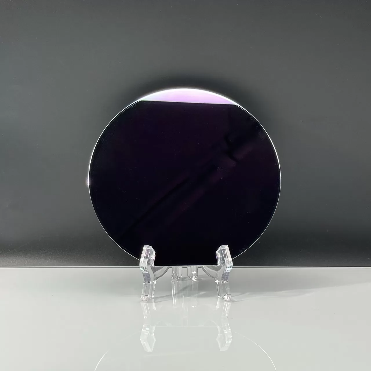
- material: high purity fused silica
- diameter: 200.0 ± 0.3 mm(Customizable)
- cte: 0.57 ppm/K
- thickness tolerance: ± 10 μm
- edge exclusion: 6 mm
- polishing: double side polished
- bow: < 80 µm
- notch: SEMI
- surface roughness (Ra): < 0.5 nm
- ttv: < 10 μm
- scratch-dig: 20-10
- cte: 0.57 ppm/K
- packaging: cleanroom packed
- packing units: 10 pcs, 25 pcs
Q&A
What is high-purity silicon?
High-purity polycrystalline silicon (polysilicon) is the starting material for nearly all semiconductors, and is the largest dollar volume chemical consumed by the electronics industry.
What are 3 types of silicon wafers?
The choice of silicon wafer depends on the application. Single crystal wafers are the most common choice for ICs, while polycrystalline wafers are often used for solar cells and LEDs. Amorphous silicon wafers are less common, but they are sometimes used for applications where cost is a major consideration.
- Monocrystalline Silicon Wafers:
- Monocrystalline silicon wafers are made from a single, continuous crystal structure, resulting in high purity and uniformity.
- They offer superior electrical properties and are often used in high-performance semiconductor devices such as microprocessors and memory chips.
- Polycrystalline Silicon Wafers:
- Polycrystalline silicon wafers are composed of multiple smaller crystals, resulting in lower purity and slightly reduced electrical performance compared to monocrystalline wafers.
- They are more cost-effective to produce and are commonly used in applications where strict performance requirements are not critical, such as solar cells and display panels.
- Epitaxial Silicon Wafers:
- Epitaxial silicon wafers are monocrystalline wafers with an additional layer of single-crystal silicon grown on the surface using a process called epitaxy.
- This layer, known as the epitaxial layer, is carefully controlled to achieve specific electrical properties, making epitaxial wafers suitable for specialized semiconductor applications requiring precise doping profiles or device isolation.