InP wafers VGF CZ Growth method N-type S doped P type Zn doped EPI-ready 2、3、4、6inch semiconductor materials
- +86138-1617-9243
- [email protected]

Focus on the field of new material !

Indium Phosphide (InP), with CAS No. 22398-80-7 and a melting point of 1600°C, belongs to the III-V family of binary compound semiconductors. It possesses a face-centered cubic crystal structure known as “zinc blende,” which is common among III-V semiconductors. InP is synthesized from high-purity indium and phosphorus elements, typically with purities of 6N to 7N, and grown into single crystals using techniques such as Liquid Encapsulated Czochralski (LEC) or Vertical Gradient Freeze (VGF).
Indium Phosphide crystals can be doped to exhibit n-type, p-type, or semi-insulating conductivity, making them suitable for further fabrication into wafers up to 6 inches (150 mm) in diameter. This semiconductor material is characterized by its direct band gap, excellent electron and hole mobility, and efficient thermal conductivity.
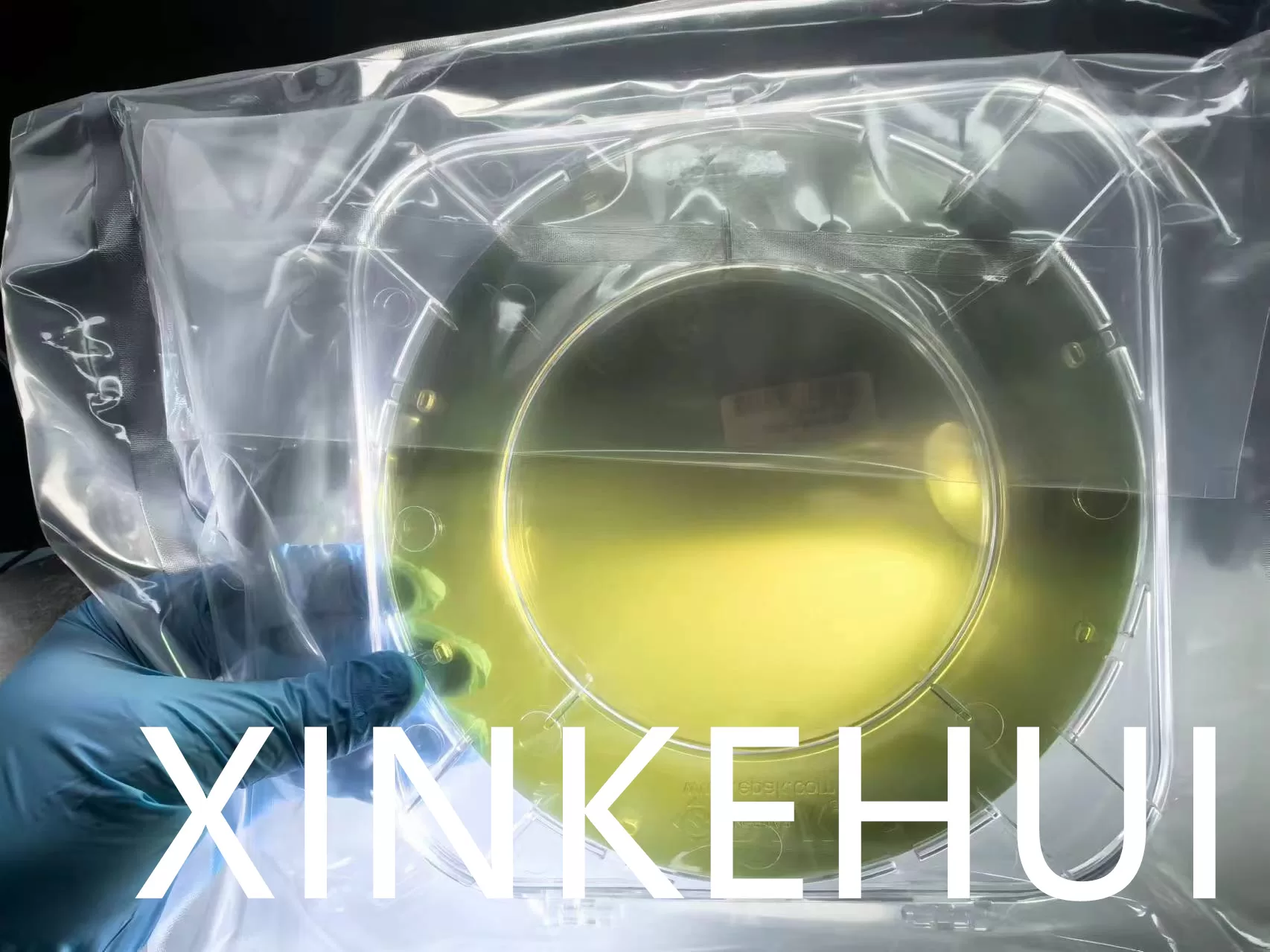
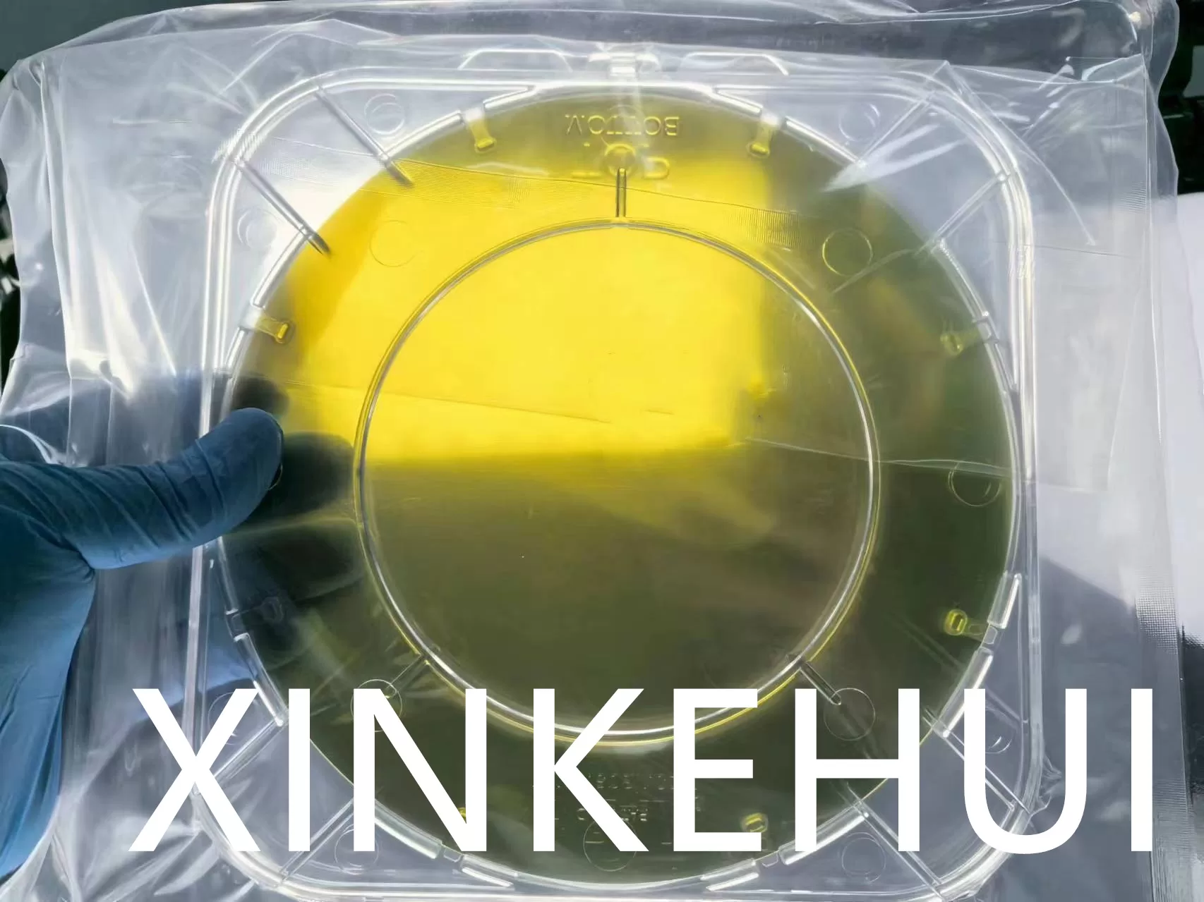
At Western Minmetals (SC) Corporation, prime or test grade Indium Phosphide (InP) wafers are available with p-type, n-type, or semi-insulating conductivity. These wafers come in sizes ranging from 2 to 6 inches (up to 150 mm) in diameter, with orientations of <111> or <100>, and thicknesses ranging from 350 to 625 micrometers. Surface finishes include etched and polished or Epi-ready processes. Additionally, single crystal ingots of Indium Phosphide in sizes from 2 to 6 inches can be provided upon request.
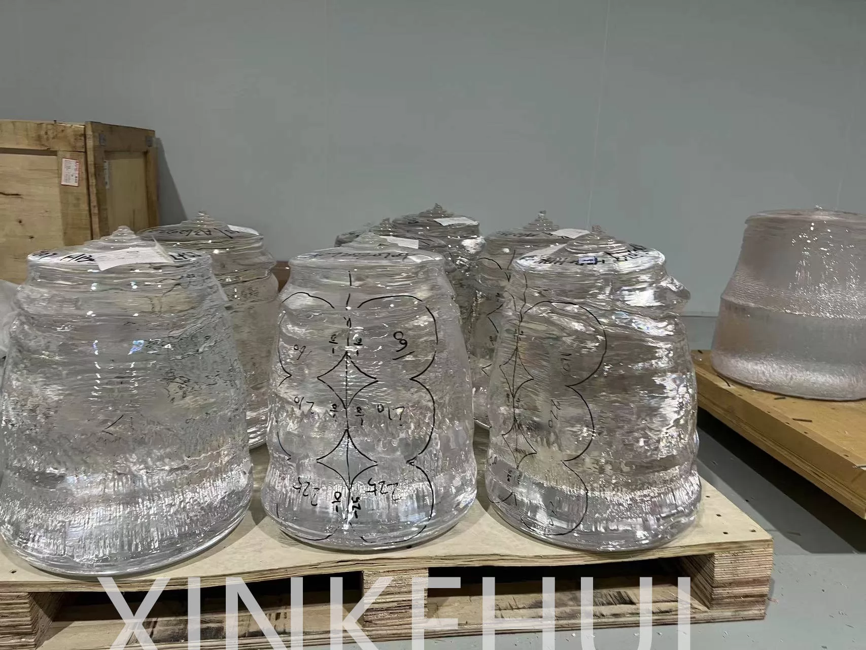
For customers seeking polycrystalline or multi-crystal Indium Phosphide (InP) ingots, options include dimensions of diameter (60-75) x length (180-400) mm and weights ranging from 2.5 to 6.0 kg. These ingots have carrier concentrations of less than 6E15 or between 6E15 and 3E16. Customized specifications are available upon request to meet specific application requirements.
| Type | Semi-Insulated | N-Type | P-Type | NP Type |
| Dopant | Fe | S, Sn | Zn | Undoped |
| Growth Method | VGF | |||
| Diameter | 2″, 3″, 4″, 6″ | |||
| Orientation | (100)±0.5° | |||
| Thickness (µm) | 350-675um ±25um | |||
| OF/IF | US EJ | |||
| Carrier Concentration | – | (0.8-8)*1018 | (0.8-8)*1018 | (1-10)*1015 |
| Resistivity (ohm-cm) | >0.5*107 | – | – | – |
| Mobility (cm2/V.S.) | >1000 | 1000-2500 | 50-100 | 3000-5000 |
| Etch Pitch Density (/cm2) | <5000 | <5000 | <500 | <500 |
| TTV [P/P] (µm) | <10 | |||
| TTV [P/E] (µm) | <15 | |||
| Warp (µm) | <15 | |||
| Surface Finished | P/P, P/E, E/E | |||

| Diameter | 2″, 3″,4″,6″,8″ |
| Thickness | 100um, 200um, 300 um, 400 um, 500 um |
| Type | P type, N type |
| Dopant | Undopped, S, Fe, Zn |
| Polishing | SSP, DSP |
| Orientation | <100> |


Indium Phosphide (InP)InP wafers stands out as a pivotal III-V compound semiconductor, representing a novel generation of electronic materials post the era of Silicon (Si) and Gallium Arsenide (GaAs). Its distinctive characteristics include a melting point soaring to 1335 + 7 Kelvin, requiring high-pressure extraction from 27.5 atmospheres. Consequently, synthesizing polycrystalline InP proves challenging, with crystal growth presenting even greater hurdles due to the perpetually high-temperature, high-pressure environment.
Moreover, InP crystals are notoriously elusive to obtain, with single crystal growth under such conditions exacerbating thermal stresses, rendering wafer processing complex. Additionally, InP’s susceptibility to stacking faults and twinning further complicates the production of high-quality crystals. Consequently, InP polishing currently commands a premium of 3 to 5 times higher than GaAs in equivalent areas. Despite these challenges, research into InP materials remains considerably less comprehensive than that of Si, GaAs, and other counterparts.
In terms of performance, InP wafers demonstrates superiority over GaAs in several respects, particularly in applications requiring high-speed and high-frequency characteristics. Its electron peak drift speed surpasses that of GaAs under high electric fields, making it a prime candidate for ultra-high-speed and ultra-high-frequency device fabrication. Moreover, InP boasts a direct transition bandgap of 1.35 electron volts, aligning with the lowest transmission loss band in optical fiber communications. Additionally, InP exhibits enhanced thermal conductivity and heat dissipation efficiency compared to GaAs, bolstering its suitability for continuous-wave (CW) device manufacturing.
In device fabrication, InP offers notable advantages over GaAs. Notably, InP devices tout higher current peak-valley ratios, translating to heightened conversion efficiency vis-à-vis GaAs counterparts. Its inertia energy time constant, merely half that of GaAs, enables InP devices to operate at twice the frequency limit. Furthermore, InP’s superior thermal conductivity lends itself to better noise characteristics in InP-based devices.
InP wafers finds widespread application as a substrate material across various sectors. In the realm of photoelectric devices, encompassing light sources (LEDs, LDs) and detectors (PDs, APDs), InP plays a pivotal role in optical fiber communication systems. InP’s bandwidth, measured at 1.34 electron volts, facilitates the production of high-efficiency and radiation-resistant solar cells, crucial for space satellite applications. Electronic devices leveraging InP, such as high-speed, high-frequency microwave devices and image sensors, find utility in millimeter-wave communication, anti-collision systems, and other emerging fields.
While current utilization of InP microwave devices and circuits predominantly targets military applications, ongoing technological advancements herald a broader transition towards civilian and dual-use applications, underscoring InP’s promising developmental trajectory and boundless potential.
Indium Phosphide (InP) has emerged as an indispensable semiconductor material for optoelectronic and microelectronic devices. In this article, we will provide a detailed overview of the preparation and industrial status of InP single crystal substrates.
I. Introduction to InP Properties
Indium Phosphide (InP) is a compound semiconductor material with a zinc blende crystal structure, characterized by its soft and brittle texture and silver-gray luster. With a melting point of 1335±7 Kelvin and a phosphorus saturation vapor pressure of 27.5 atmospheres near its melting point, synthesizing InP polycrystals via melt-based methods proves challenging, while alternative methods incur higher costs. Compared to Si and GaAs materials, InP exhibits high efficiency in electro-optical conversion, high electron mobility, elevated operating temperatures, robust radiation resistance, and excellent thermal conductivity.
InP finds widespread application in fields such as terahertz (THz) technology, lasers, solar cells, photodetectors, and optical fiber network systems, including last-mile fiber and data center transmissions.
II. Methods for InP Polycrystal Preparation
Several methods exist for synthesizing InP polycrystalline materials, including Horizontal Bridgman (HB) and Horizontal Gradient Freeze (HGF) techniques, Solvent-Solubility-Diffusion (SSD) synthesis, and In-situ Synthesis methods involving P injection, P liquid sealing, and various modifications. Presently, the primary industrial methods for synthesizing InP polycrystals involve HB/HGF techniques.
Horizontal Bridgman (HB) / Horizontal Gradient Freeze (HGF) Overview:
InP polycrystals are synthesized by reacting phosphorus vapor with molten indium. When the temperature of the indium melt exceeds the melting point of InP, phosphorus vapor is absorbed by the indium melt until the entire indium melt is transformed into InP melt.
III. InP Single Crystal Growth Technology
The growth of InP single crystals involves the transition of a liquid phase to a solid phase, constituting a phase change process. Single crystal growth can be categorized into vertical and horizontal growth methods. Commonly used single crystal growth methods include Liquid Encapsulated Czochralski (LEC), Modified LEC, Vapor Pressure Control LEC (VCz or PC-LEC, also known as Hot-Wall Cz HW-Cz), Vertical Gradient Freeze (VGF), Vertical Bridgman (VB), Horizontal Gradient Freeze (HGF), and Horizontal Bridgman (HB) techniques. In crystal preparation, critical technologies include thermal field design and twin control. From a technological and cost perspective, LEC technology is the primary method for producing large-sized crystals, while VGF/VB methods are used to produce low-dislocation substrates.
IV. Substrate Types
InP substrates are primarily categorized based on their electrical conductivity into semiconductor and semi-insulating substrates.
Semiconductor substrates are further divided into N-type and P-type semiconductor substrates. Typically, In2S3 and Sn are used as dopants for N-type substrates, while ZnP2 is used for P-type substrates. Various dopants are employed to provide different conductivity types for device manufacturing.
N-type doping with Sn in InP is mainly used for laser diodes. N-type doping with S in InP is used not only for laser diodes but also for photodetectors, with the necessity of defect-free doping for avoiding leakage currents generated by dislocations. Therefore, dislocation-free doping is essential, and since sulfur has a significant impurity hardening effect in InP, dislocation-free single crystals can be easily grown. P-type doping with Zn in InP is primarily used for high-power laser diodes. Zn also has a strong impurity hardening effect, thereby reducing dislocations. Low dislocation levels are crucial for improving the lifetime of lasers.
Semi-insulating substrates are categorized based on whether they are doped or undoped. Doped semi-insulating substrates typically use Fe2P as a dopant, while undoped semi-insulating substrates are obtained by high-temperature annealing of high-purity InP single crystal substrates. Semi-insulating substrates are primarily used in RF device manufacturing.
A trialkyl indium molecule and phosphide mixture can similarly be thermally decomposed to form indium phosphide. Because of its better electron velocity than the more popular semiconductors silicon and gallium arsenide, inP is utilized in high-power and high-frequency circuits.
InP wafers are semiconductor substrates made from indium phosphide (InP) material. These wafers are used as a platform for the fabrication of electronic and optoelectronic devices. InP wafers offer unique properties suitable for a wide range of applications, including high-speed transistors, photodetectors, lasers, solar cells, and integrated circuits.
The fabrication process typically involves growing a single crystal of InP material and then slicing it into thin wafers. These wafers undergo various processing steps, such as polishing, doping, and patterning, to create the desired electronic or optoelectronic devices. InP wafers are characterized by their high electron mobility, direct bandgap, and excellent thermal conductivity, making them well-suited for applications requiring high-performance semiconductor materials.
Indium phosphide (InP) refers to a binary semiconductor that consists of indium (In) and phosphorus (P). Like gallium arsenide (GaAs) semiconductors that come with a zincblende crystal structure, InP is classified under a group of materials that belong to the III-V semiconductors.
InP semiconductor refers to indium phosphide, a compound semiconductor material composed of indium (In) and phosphorus (P) atoms. InP is part of the III-V semiconductor family, which includes materials formed from elements in groups III and V of the periodic table.
Indium phosphide (InP) possesses unique electronic and optical properties that make it suitable for a wide range of applications in the semiconductor industry. Some key characteristics of InP semiconductor include:
Overall, InP semiconductor materials play a crucial role in various industries, including telecommunications, aerospace, solar energy, and consumer electronics, due to their unique combination of electronic and optical properties.
Indium phosphide (InP) is a binary semiconductor composed of indium and phosphorus. It has a face-centered cubic (“zincblende”) crystal structure, identical to that of GaAs and most of the III-V semiconductors.
Indium phosphide (InP) wafer are manufactured by the reaction of indium iodide and white phosphorus at the temperature of 400 °C. In addition, it can also be manufactured by integrating the clean components at high pressure and high temperature.
Aluminum Nitride (AlN) is increasingly recognized as a pivotal material in the realm of advanced technological applications, particularly where superior thermal management and electrical insulation are paramount. With its unparalleled thermal conductivity of 170 W/mK, Aluminum Nitride (AlN) Substrate stands as the epitome of thermally conductive materials that also possess robust electrical insulating properties. This unique combination renders it an indispensable resource in various high-demand applications, especially those requiring efficient heat dissipation away from critical components.
The OCTO brand, known for its quality and innovation, offers blank aluminum nitride substrates that cater to a wide array of needs in the technology and manufacturing sectors. These substrates are not just any materials; they are the backbone of heat management in sophisticated devices. Available in various sizes and thicknesses, they are designed to meet the stringent requirements of today’s high-power, high-performance components. Whether it’s power LEDs, high-power integrated circuits (ICs), or high-voltage inductors, Aluminum Nitride (AlN) Substrate from OCTO provide the foundation for reliability and efficiency.


Silicon wafers are indispensable in semiconductor manufacturing for electronic devices. Their versatility in shape and abundant availability make them a preferred choice. This study explores the benefits of silicon wafer manufacturing, which involves molding them into various shapes like cylinders or squares. The process encompasses multiple steps, ensuring high-quality results.
The primary flat of a silicon wafer, known as the primary flat, determines the crystal orientation, with secondary and quaternary planes characterized by doping levels and orientations. In silicon, the smallest crystal is designated as (100), with the primary flat being the longest and largest. The secondary facets, cut in the R-plane, indicate the doping level.
Silicon wafer properties are classified by type, with intrinsic wafers being pure silicon and P-types characterized by electrons. These properties significantly influence the electrical response of devices. Moreover, the polarity of a silicon ingot impacts semiconductor processing techniques, such as etching and ion implantation. Polishing follows ingot shaping in the fabrication process.