Silicon Wafer’s abstract
Silicon wafers are indispensable in semiconductor manufacturing for electronic devices. Their versatility in shape and abundant availability make them a preferred choice. This study explores the benefits of silicon wafer manufacturing, which involves molding them into various shapes like cylinders or squares. The process encompasses multiple steps, ensuring high-quality results.
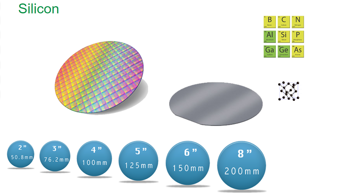
The primary flat of a silicon wafer, known as the primary flat, determines the crystal orientation, with secondary and quaternary planes characterized by doping levels and orientations. In silicon, the smallest crystal is designated as (100), with the primary flat being the longest and largest. The secondary facets, cut in the R-plane, indicate the doping level.
Silicon wafer properties are classified by type, with intrinsic wafers being pure silicon and P-types characterized by electrons. These properties significantly influence the electrical response of devices. Moreover, the polarity of a silicon ingot impacts semiconductor processing techniques, such as etching and ion implantation. Polishing follows ingot shaping in the fabrication process.
Silicon Wafer’s showcase
Silicon Wafer’s properties(partly)
- Material: Single Crystal Silicon Wafer
- Growth Method: MCZ
- Orientation: <100>
- Diameter: 100 mm +/- 0.5 mm
- Thickness: 525 um +/- 25 um (SSP)
- Primary Flat Orientation: <110> +/-1 deg
- Primary Flat Length: 32.5 +/- 2.5 mm
- Secondary Flat Orientation: 90 deg from primary flat
- Secondary Flat Length: 18.0 +/- 2.0 mm
- Type/ Dopant: P/ Boron
- Thermal Expansion Coefficient: 2.6·10-6°C -1
- Electrical Resistivity: 10-20 ohm-cm
- RRV: 8% (6mm)
- Oxygen Content: 1.6 x 10^18 atoms/cm3
- Carbon Content: 0.5 ppm
- GBIR/ TTV: 5 µm
- WARP: 30 µm
- BOW: 30 µm
- Front Surface: CMP Polished, Ra < 0.5 nm (single side polished, SSP)
- Package: Packaged in a class 100 clean room environment, in cassettes of 25 wafers.
- Material: Single Crystal Silicon Wafer
- Growth Method: MCZ
- Orientation: <100>
- Diameter: 100 mm +/- 0.5 mm
- Thickness: 525 um +/- 20 um (SSP)
- Primary Flat Orientation: <110> +/-1 deg
- Primary Flat Length: 32.5 +/- 2.5 mm
- Secondary Flat Orientation: 90 deg from primary flat
- Secondary Flat Length: 18.0 +/- 2.0 mm
- Type/ Dopant: P/ Boron
- Thermal Expansion Coefficient: 2.6·10-6°C -1
- Electrical Resistivity: 10-20 ohm-cm
- RRV: 8% (6mm)
- Oxygen Content: 1.6 x 10^18 atoms/cm3
- Carbon Content: 0.5 ppm
- GBIR/ TTV: 5 um
- WARP: 30 um
- BOW: 30 um
- Front Surface: CMP Polished, Ra < 0.5 nm (single side polished, SSP)
- Package: Packaged in a class 100 clean room environment, in cassettes of 25 pcs under vacuum or in single wafer containers.
- Purity: Silicon wafers are typically made from highly pure silicon, ensuring minimal impurities that could affect device performance.
- Crystal Structure: Silicon wafers have a crystalline structure, with the orientation of the crystal lattice influencing their electrical properties.
- Doping: Doping is the process of intentionally introducing impurities into the silicon lattice to alter its electrical conductivity. Silicon wafers can be doped with specific elements to create P-type (positively charged) or N-type (negatively charged) regions, enabling the fabrication of various semiconductor devices.
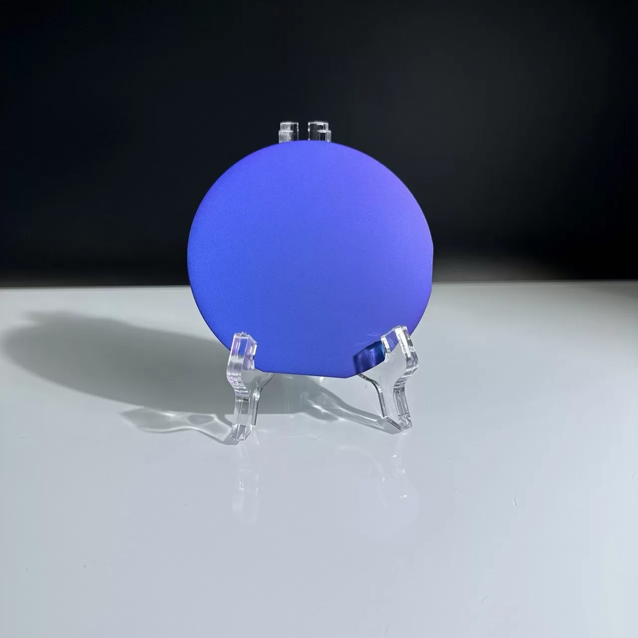
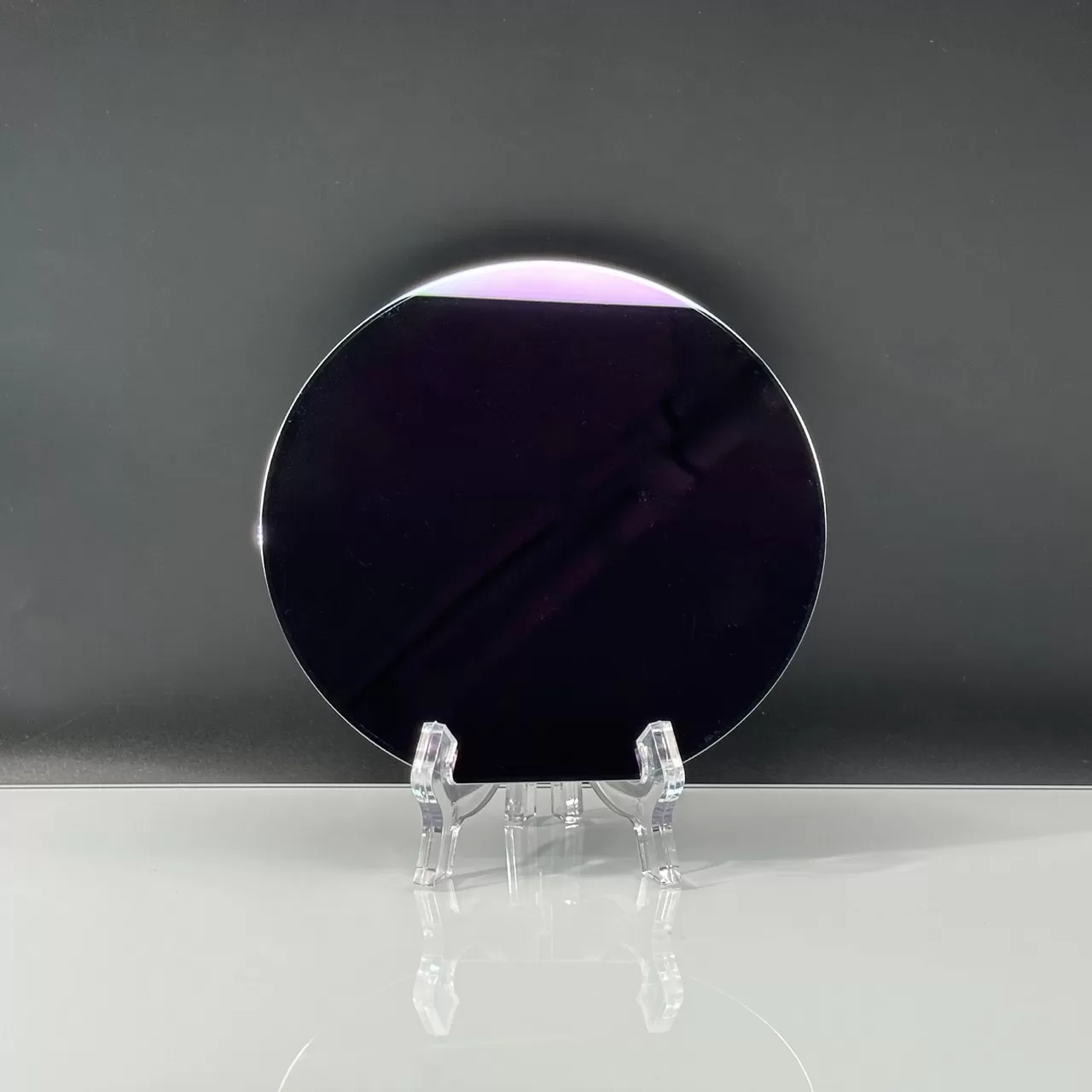
- Size and Shape: Silicon wafers come in various sizes, commonly ranging from 2 inches to 12 inches in diameter. They can be molded into different shapes, such as circular or square, to accommodate different manufacturing processes.
- Surface Finish: The surface of silicon wafers is typically polished to achieve a high degree of flatness and smoothness, ensuring uniformity in device fabrication.
- Thickness: Silicon wafers are available in different thicknesses, ranging from a few micrometers to several hundred micrometers, depending on the specific application requirements.
- Thermal Conductivity: Silicon wafers exhibit high thermal conductivity, allowing for efficient dissipation of heat generated during device operation.
- Optical Properties: Silicon wafers are transparent to infrared radiation, making them suitable for applications in infrared sensors and detectors.
Silicon Wafer’s application
- Integrated Circuits (ICs): Silicon wafers are the foundational material for manufacturing ICs, which are essential components in electronic devices such as computers, smartphones, and automotive electronics.
- Solar Cells: Silicon wafers are used in the production of solar cells for photovoltaic panels, converting sunlight into electricity in residential, commercial, and industrial settings.
- MEMS Devices: Microelectromechanical systems (MEMS) devices, including accelerometers, gyroscopes, and pressure sensors, often utilize silicon wafers as the substrate due to their compatibility with semiconductor fabrication processes.
- Optoelectronics: Silicon wafers are employed in the production of optoelectronic devices such as light-emitting diodes (LEDs), photodiodes, and optical switches used in telecommunications, lighting, and sensing applications.
- Power Devices: Silicon wafers serve as the base material for manufacturing power semiconductor devices like diodes, thyristors, and insulated gate bipolar transistors (IGBTs), used in power electronics applications such as motor drives, inverters, and power supplies.
- Microfluidics: Silicon wafers are utilized in microfluidic devices for biomedical applications, such as lab-on-a-chip systems for drug delivery, DNA analysis, and point-of-care diagnostics.
- Wafer Bonding: Silicon wafers are bonded with other materials (e.g., glass, polymers) using various techniques to create advanced structures for applications in microelectronics, optics, and micro-electro-mechanical systems (MEMS).
- Semiconductor Wafer Test: Silicon wafers are used as substrates for testing semiconductor devices during the manufacturing process to ensure their quality and functionality before integration into electronic systems.
- Semiconductor Packaging: Silicon wafers are utilized as carrier substrates for packaging semiconductor chips into various forms such as flip-chip, wire-bond, and ball-grid array (BGA) packages, enabling their integration into electronic products.
- Research and Development: Silicon wafers serve as essential materials for research and development in academia, government laboratories, and industry, enabling the exploration of new technologies and the advancement of semiconductor science and engineering.
Manufacturing Process
Silicon wafers are crucial components in the manufacturing process of electronic devices such as cell phones, TVs, computers, and smart speakers.
These wafers are thin slices of pure crystallized silicon, often referred to as undoped or intrinsic silicon wafers. One of the primary reasons for using silicon wafers in the semiconductor industry is the abundance of silicon in nature. It is one of the most abundant materials on Earth, usually found in the form of SiO2. Another reason for using silicon is its controllable electrical characteristics through the addition of dopants. Doping with impurities such as Boron creates P-type wafers, while doping with Arsenic or Phosphorous creates N-type wafers. P-type wafers contain positively charged holes, whereas N-type wafers contain negatively charged electrons.
The history of electronic device/component manufacturing dates back to vacuum tubes, which were eventually replaced by solid-state transistors made of Germanium. The first integrated circuit (IC) was developed in 1959 by Jack Kilby at Texas Instruments, based on Germanium. However, modern ICs based on silicon were pioneered by Robert Noyce at Fairchild Camera, leveraging silicon’s advantages, such as the use of SiO2 as an insulating/dielectric layer to create MOSFETs and evaporated aluminum for electrical connections, leading to the creation of monolithic ICs, where all electronic components are on the same wafer.
Over the decades, advancements in IC manufacturing have seen improvements in process technology, resulting in smaller feature sizes (e.g., 10nm, 7nm, 5nm) and structural improvements, such as the transition from planar to tri-gate transistor architecture for higher performance. Additionally, the size of silicon wafers has increased from 50mm in the 1970s to 300mm today, enabling denser integration (VLSI) but requiring upgrades to fabrication facilities.
The IC manufacturing process can be broadly categorized into material preparation (from sand to poly Silicon), wafer preparation (from poly Silicon to Silicon wafer), wafer fabrication and sorting of integrated circuits, packaging, and electrical testing. The initial steps involve obtaining pure single crystal Silicon from quartzite through a reduction process in a submerged electrode arc furnace, yielding metallurgical grade silicon with minor impurities.
The purity and crystalline structure of silicon wafers play a critical role in the performance and reliability of electronic devices, making them indispensable in modern technology.
SiC + SiO2 ——-> Si + SiO + CO
The temperature of the process is high enough to get Silicon in molten form which is separated easily. This Silicon, normally referred as metallurgical grade silicon, is 98% pure form of Silicon with minor Aluminum and Iron impurities.
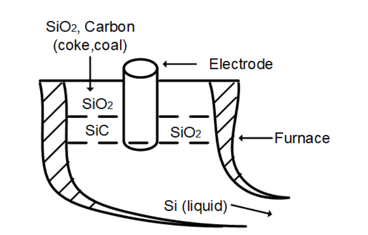
Figure 1: Metallurgical Grade Silicon Extraction
The next step involves purifying the extracted silicon through a fractional distillation process. In this process, silicon reacts with hydrochloric gas in a reactor at around 300 degrees Celsius.
Si + 3HCl → SiHCl3 + H2
The SiHCl3 gas is then separated by fractional distillation and reduced using hydrogen gas.
2SiHCl3 + 2H2 → 2Si + 6HCl
This process can be repeated multiple times to obtain a more purified form of silicon, known as electronic grade silicon. However, electronic grade silicon remains polycrystalline rather than a single crystal of silicon. Therefore, the next step is to convert this purified silicon into a single crystal wafer.
One of the predominant methods for producing single crystal silicon from polycrystalline silicon is the Czochralski growth method. This method accounts for 80-90% of the wafers used in fabrication labs.
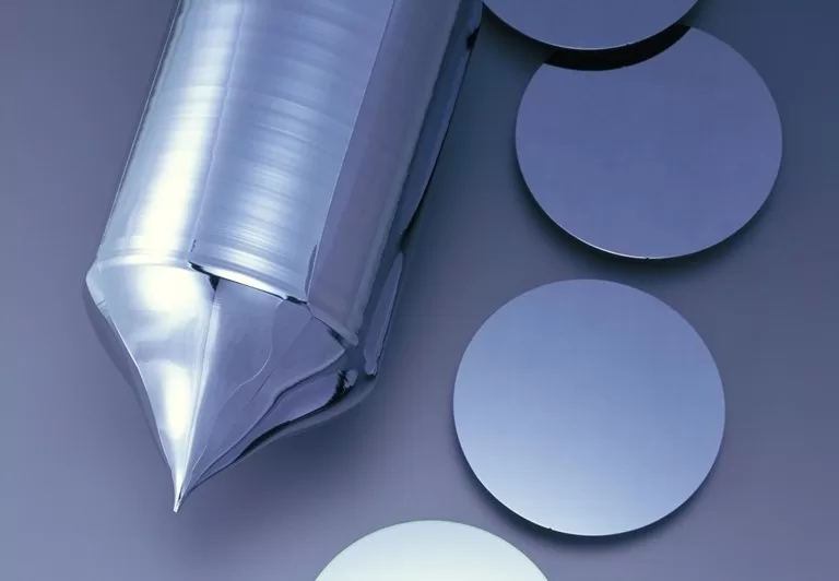
In the Czochralski growth method, pure silicon is melted in a furnace heated by RF coils at around 1500 degrees Celsius. A seed crystal with the correct orientation is then placed on a rotor and dipped into the molten silicon. The seed silicon is slowly withdrawn from the molten silicon with rotation. As the seed crystal is withdrawn, molten silicon attaches to it and adopts the same orientation as the seed crystal when it cools down. The rotation during withdrawal ensures the creation of a uniform cylindrical silicon piece.
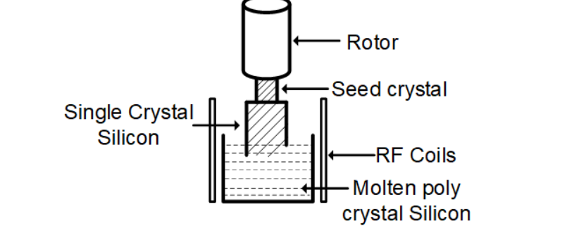
Figure 2: Czochralski Method
After the single crystal silicon is created, it undergoes shaping and cutting processes. Industrial diamond tools are utilized for this purpose. The seed crystal is removed from the generated single crystal silicon, and surface grinding is performed to enhance smoothness. Subsequently, flats are ground onto the silicon along the lengths of the wafers. These flats, known as primary flat or secondary flat, are associated with crystal orientation and serve for identification and sorting purposes.
Different types of silicon wafers are ground with different flats. For instance, a P-type wafer with an orientation of 111 has only one primary flat, whereas an N-type wafer with the same orientation has one primary and one secondary flat. Similarly, both P[100] and N[100] wafers have primary and secondary flats, albeit with different angles to each other.
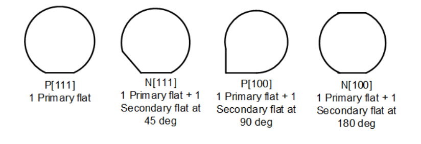
Figure 3: Silicon Wafer Flat Types
Following the grinding process, the silicon undergoes cutting to produce silicon wafers, utilizing industrial-grade diamond tools for slicing. Subsequently, the created wafers are subjected to a chemical etching process to eliminate any damage and contaminated regions on their surfaces.
Next, the wafers undergo polishing, which can be either single-sided or double-sided, although single-sided polishing is more prevalent. Once polished, these wafers are deemed ready for use in the fabrication lab.
Q&A
Which Si Wafer Should I Use for My Research?
An Si wafer serves as a vital semiconductor material, primarily utilized in the production of microchips for electronic devices. Given silicon’s abundance, it is the preferred choice for manufacturing these components. Si wafer manufacturing offers several advantages. These wafers are highly versatile and can be shaped into various forms, including cylinders or squares. The manufacturing process involves several intricate steps, but the resulting product justifies the effort.
The primary flat of a silicon wafer, known as the primary flat, plays a crucial role. Its orientation determines the crystal structure’s polarity. Secondary and quaternary planes are distinguished by their doping levels and orientations. In silicon, the smallest crystal is denoted as (100), with the primary flat being the longest and largest. Secondary facets are cut in the R-plane and provide insights into the doping level.
Silicon wafers exhibit distinct physical and electrical properties based on their type. Intrinsic wafers consist of pure silicon, while P-type wafers are characterized by electrons. These characteristics significantly impact the electrical behavior of devices. The polarity of a silicon ingot influences semiconductor processing techniques, such as etching and ion implantation. Following ingot shaping, the subsequent fabrication step involves polishing the wafer to ensure smoothness and uniformity.
What is a silicon wafer used for?
Silicon wafers are the semiconductors that are utilized for manufacturing microchips and chips in electronic devices. Integrated circuits are built by these semiconductors due to the features of the current of electricity through silicon wafers.
What are 3 types of silicon wafers?
UniversityWafer, Inc. carries all types of silicon wafers. Including undoped, boron, gallium, arsenic and antimony doped.
How does a silicon wafer become a chip?
Microchips are made layer-by-layer on a silicon wafer using a process called photolithography. Light, gases, and chemicals are used to create the chip layers. The wafer is then bombarded with atoms to adjust its conductivity. Aluminum foil is then used to create conducting pathways in the wafer.