Focus on the field of new material !

6 Inch N Type Polished Silicon Wafer in hot demand

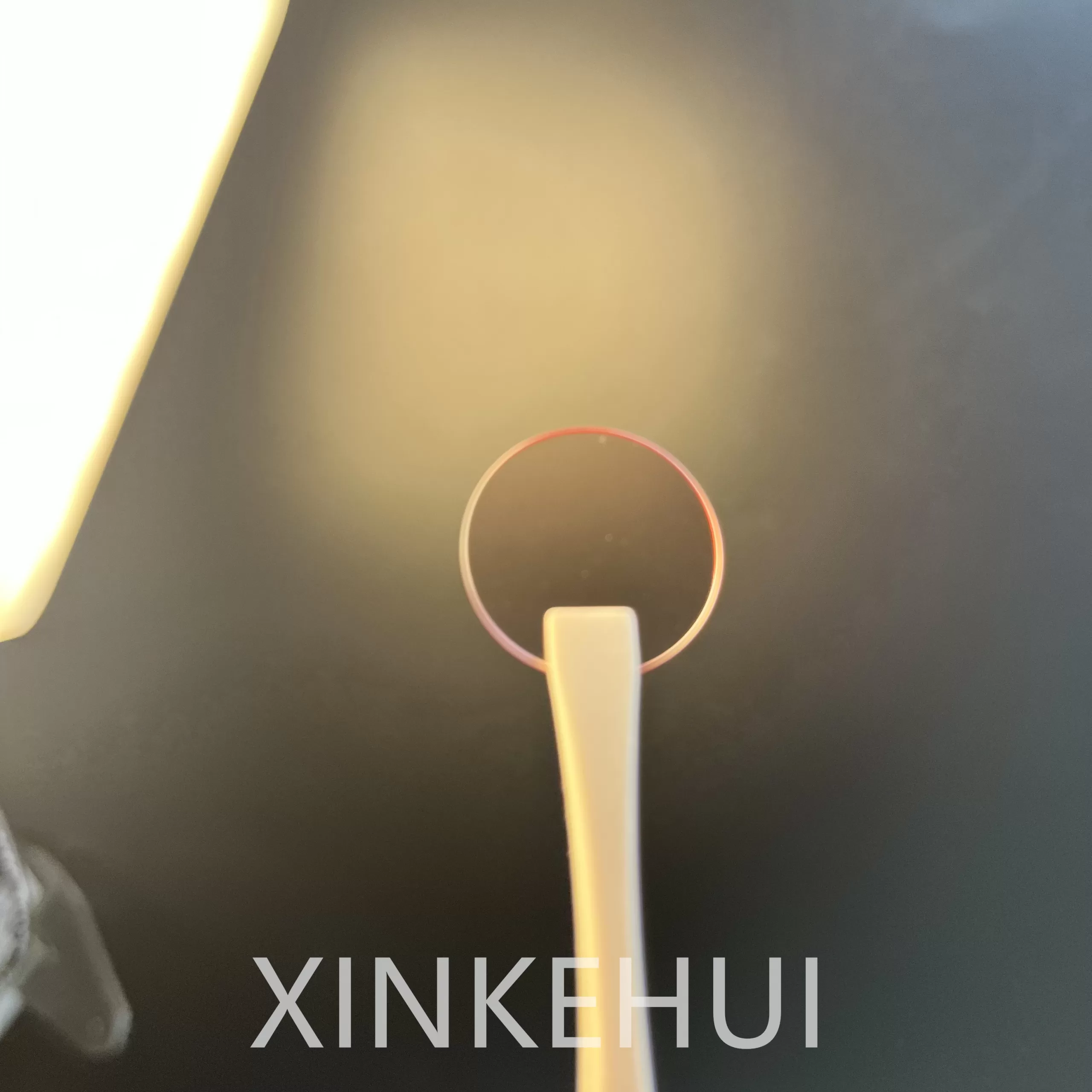
    A silicon wafer, commonly referred to as Si wafer, is a fundamental component in the field of semiconductor manufacturing. This thin and disc-shaped slice is typically made from single-crystal silicon and plays a pivotal role in the production of integrated circuits (ICs) and microelectronic devices.

    They are engineered with precision, and their properties are crucial for ensuring the performance and reliability of electronic components. These wafers serve as the foundational substrate for the fabrication of semiconductor devices that power a wide range of electronic products, from computers and smartphones to various industrial applications.

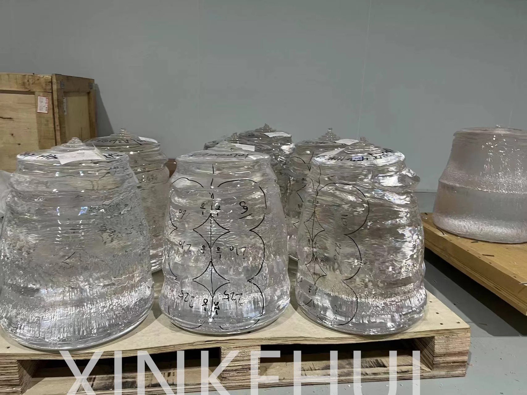
    The manufacturing process of Si wafers involves several intricate steps. Initially, high-purity silicon is melted and then solidified into a single crystal through a method called the Czochralski process. The resulting cylindrical ingot is then sliced into thin wafers using precision cutting techniques. These wafers undergo rigorous polishing to achieve a smooth and flawless surface.

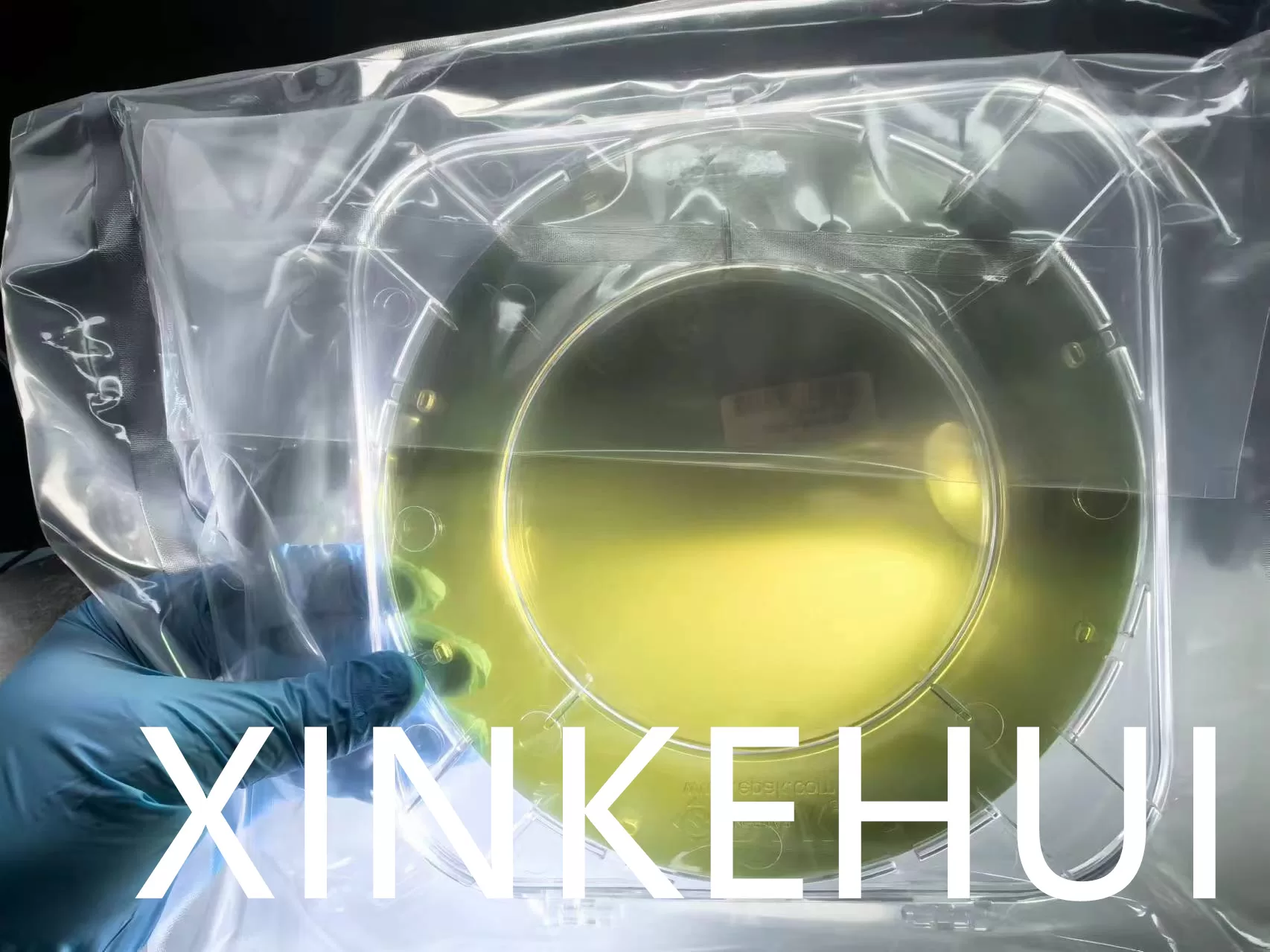
    Once the silicon wafers are prepared, they undergo various processes such as doping and lithography to introduce specific electrical properties and create intricate patterns for electronic circuits. Doping involves introducing impurities into the silicon lattice to alter its conductivity, allowing the creation of n-type and p-type regions essential for transistor operation.

    Lithography is a key step where a pattern is transferred onto the wafer’s surface using photomasks and light exposure. This process defines the intricate circuitry that constitutes the electronic components. The pattern is etched into the silicon, and layers of materials, such as metals and insulators, are deposited to build the circuitry.

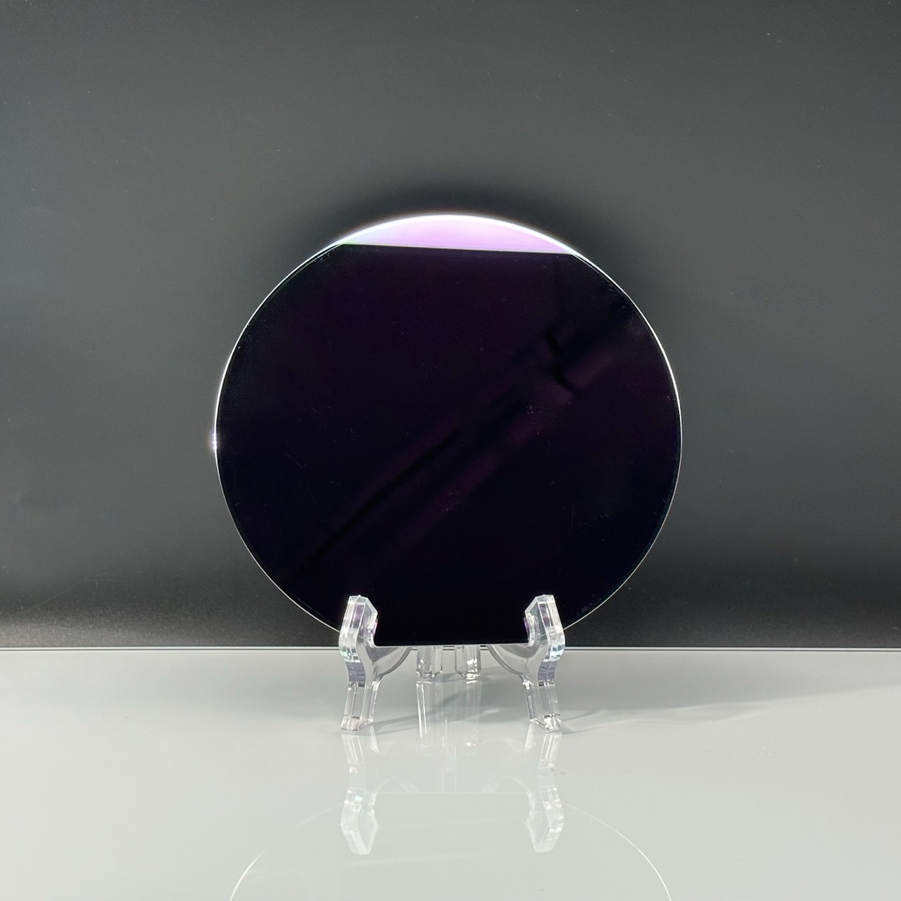
    The silicon wafer’s diameter has evolved over time, with larger wafer sizes becoming more prevalent in modern semiconductor manufacturing. Common wafer sizes include 150mm, 200mm, and 300mm, allowing for higher efficiency and increased yield in the production of electronic devices.

    they also play a crucial role in enabling the miniaturization of electronic components, as advancements in technology strive to reduce the size of transistors and enhance the overall performance of semiconductor devices.

    In conclusion, they are foundational elements in the world of semiconductor manufacturing, serving as the canvas for the intricate electronic circuits that power today’s technological landscape. The continuous advancement of silicon wafer technology contributes to the development of more powerful, efficient, and compact electronic devices.

    Silicon Wafer’s feature

    Si wafer
    Si wafer
    • Single-Crystal Structure: Silicon wafers are typically crafted from a single crystal, ensuring uniformity and reliability in electronic performance.
    • High Purity: These wafers exhibit exceptional purity, crucial for preventing impurities that can adversely affect electronic properties.
    • Precision Thickness: they are manufactured with precise thickness, a critical factor in the performance of integrated circuits.
    • Smooth Surface: Through rigorous polishing processes, they achieve a smooth and flawless surface necessary for precise lithography.
    • Diameter Variability:they come in various diameters (e.g., 150mm, 200mm, 300mm), catering to diverse manufacturing needs and efficiency.
    • Doping Capability: The silicon lattice allows for controlled doping, enabling the creation of n-type and p-type regions for transistor functionality.
    • Thermal Stability: they exhibit high thermal stability, essential for maintaining electronic performance across varying operating conditions.
    • Semiconductor Properties: As a semiconductor material, they facilitate the controlled flow of electrons, forming the basis for electronic devices.
    • Lithography Compatibility: they are compatible with precise lithography techniques, enabling the creation of intricate circuit patterns.
    • Dielectric Properties: Silicon dioxide, often used as an insulator on these wafers, provides excellent dielectric properties for isolation between components.
    • Low Defect Density: Careful manufacturing processes result in silicon wafers with low defect densities, enhancing the reliability of integrated circuits.
    • Wafer Flatness: they maintain a high degree of flatness, ensuring uniformity in the fabrication process and subsequent device performance.
    • Chemical Inertness: Silicon is chemically inert, contributing to the stability and longevity of electronic components built on silicon wafers.
    • Electron Mobility: they offer high electron mobility, a crucial factor in achieving fast and efficient electronic signal processing.
    • Photolithography Compatibility: they are well-suited for photolithography, a key step in defining intricate circuit patterns during semiconductor manufacturing.
    • Low Electronic Noise: Silicon’s inherent properties contribute to low electronic noise levels, enhancing the signal-to-noise ratio in electronic devices.
    • Oxidation Resistance: they exhibit resistance to oxidation, maintaining their integrity over extended periods of use.
    • Wafer Flexibility: they provide flexibility in design and manufacturing processes, adapting to evolving semiconductor technologies.
    • High Breakdown Voltage: Silicon’s high breakdown voltage makes it suitable for power devices, contributing to the robustness of electronic components.
    • Widespread Industry Adoption: they are widely adopted in the semiconductor industry, underlining their significance in electronic device manufacturing.
    Si wafer
    Si wafer

    Silicon Wafer’s application

    1. Integrated Circuits (ICs): Silicon wafers form the basis for manufacturing ICs, the core components in electronic devices.
    2. Microprocessors: Used in the production of microprocessors that power computers, servers, and other computing devices.
    3. Memory Devices: Silicon wafers are crucial for creating memory devices like RAM and flash memory.
    4. Microcontrollers: Applied in the fabrication of microcontrollers used in various electronic systems.
    5. Power Devices: they play a role in manufacturing power devices for energy management and distribution.
    6. Transistors: Form the foundation for transistor manufacturing, essential in electronic switching.
    7. Sensors: Utilized in sensor technology for applications ranging from automotive to industrial sensing.
    8. Photovoltaic Cells: Silicon wafers are key components in the production of solar cells for renewable energy.
    9. Radio-Frequency (RF) Devices: Applied in RF devices for wireless communication and signal processing.
    10. Optoelectronics: Used in the production of optoelectronic devices like light-emitting diodes (LEDs) and photodetectors.
    11. MEMS (Micro-Electro-Mechanical Systems): they are employed in the fabrication of MEMS devices for sensing and actuation.
    12. Analog Circuits: Essential for creating analog circuits for signal processing and amplification.
    13. Logic Circuits: Silicon wafers are integral in the manufacture of logic circuits for digital processing.
    14. Power Amplifiers: Used in the production of power amplifiers for various electronic applications.
    15. Microfabrication: Silicon wafers enable microfabrication processes for creating intricate structures on a small scale.
    16. Biomedical Devices: Applied in the production of biomedical devices for diagnostics and monitoring.
    17. Microscale Heat Exchangers: Utilized in microscale heat exchangers for thermal management in electronics.
    18. Inertial Navigation Systems: Silicon wafers contribute to the manufacturing of inertial navigation systems for precise navigation.
    19. Microfluidic Devices: Used in the fabrication of microfluidic devices for precise fluid control.
    20. Consumer Electronics: Silicon wafers are pervasive in consumer electronics, including smartphones, tablets, and smartwatches.
    21. Printed Circuit Boards (PCBs): Integral to the production of PCBs, serving as the foundation for electronic components.
    22. Wireless Communication Devices: Silicon wafers play a role in the production of devices for wireless communication, such as Wi-Fi modules.
    23. Automotive Electronics: Applied in various automotive electronic components, including engine control units and sensors.
    24. Digital Signal Processors (DSPs): Silicon wafers contribute to the manufacturing of DSPs for signal processing applications.
    25. Microscale Actuators: Utilized in microscale actuators for precise mechanical control in miniature systems.
    26. RFID (Radio-Frequency Identification): Silicon wafers are used in the production of RFID tags for tracking and identification.
    27. Microwave Devices: Applied in the fabrication of microwave devices for communication and radar systems.
    28. Satellite Technology: Silicon wafers play a role in manufacturing components for satellite communication and navigation.
    29. Electronic Displays: Used in the production of electronic displays, including LCDs and OLEDs.
    30. Internet of Things (IoT) Devices: Silicon wafers contribute to the production of devices for the IoT ecosystem.
    31. Medical Imaging Devices: Applied in the manufacturing of components for medical imaging devices like X-ray detectors.
    32. Semiconductor Lasers: Used in the production of semiconductor lasers for various applications, including optical communication.
    33. Automated Control Systems: Silicon wafers are integral to the development of automated control systems in industries.
    34. Electric Vehicles (EVs): Silicon wafers play a role in the manufacturing of electronic components for electric vehicles.
    35. Aerospace Electronics: Applied in aerospace electronics for avionics and control systems.
    36. Telecommunication Infrastructure: Silicon wafers contribute to the production of components for telecommunication infrastructure.
    37. Digital Cameras: Used in the manufacturing of digital camera sensors for capturing images.
    38. Microscale Resonators: Silicon wafers are employed in the production of microscale resonators for precise frequency control.
    39. Automated Manufacturing Systems: Integral to the development of electronic components in automated manufacturing.
    40. Industrial Control Systems: Silicon wafers are utilized in the fabrication of components for industrial control systems and automation.

    Parameter Table for Silicon Wafer

    silicon wafer
    silicon wafer

    Q&A

    What is a silicon wafer used for?

    Silicon wafers are the semiconductors that are utilized for manufacturing microchips and chips in electronic devices. Integrated circuits are built by these semiconductors due to the features of the current of electricity through silicon wafers.

    How does a silicon wafer become a chip?

    Microchips are made layer-by-layer on a silicon wafer using a process called photolithography. Light, gases, and chemicals are used to create the chip layers. The wafer is then bombarded with atoms to adjust its conductivity. Aluminum foil is then used to create conducting pathways in the wafer.

    What is the difference between silicon and silicon wafer?

    Quick summary. Silicon is a naturally occurring element that is commonly used to make electronics, such as microchips and circuit boards. Silicones are synthetic materials similar to rubbers that are used to make a wide variety of products, such as adhesives and lubricants.

    advisory
    Get Better Quote