
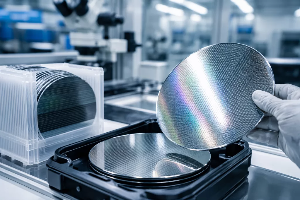
SiC wafer have become a foundational material in modern power electronics and high-frequency devices, driven by their superior physical and electrical properties. Compared with conventional silicon, SiC exhibits a wide bandgap (~3.26 eV for 4H-SiC), high thermal conductivity, and a strong critical electric field, enabling devices to operate efficiently under high voltage, high temperature, and high-frequency conditions. These advantages have accelerated the adoption of SiC in electric vehicles, renewable energy systems, industrial drives, and advanced power conversion technologies.
As application requirements become increasingly specialized, standard wafer specifications are often insufficient. In practice, device performance, yield, and long-term reliability are closely tied to substrate parameters. This has led to the growing importance of custom SiC wafer solutions, where wafer size, thickness, crystal orientation, surface quality, and doping characteristics are precisely engineered to meet specific application needs.
1. Wafer Size: Scaling for Performance and Cost
1.1 Evolution Toward Larger Diameters
The transition to larger wafer diameters is one of the most significant trends in SiC substrate development. Early-stage SiC devices were primarily fabricated on 2-inch and 4-inch wafers due to limitations in crystal growth technology. Over the past decade, 6-inch (150 mm) wafers have become the industry standard, offering a balance between manufacturability and cost efficiency.
More recently, 8-inch (200 mm) wafers have entered production, driven by the need to improve throughput and reduce cost per device. At the leading edge, 12-inch (300 mm) SiC wafers have begun to move into early-stage mass production, marking an important milestone for the industry. However, scaling to this size introduces significant technical challenges, including:
- Maintaining low defect density across a larger crystal volume
- Controlling wafer bow and residual stress
- Ensuring uniform electrical and structural properties
As a result, while 12-inch wafers represent a promising direction, further optimization in yield, uniformity, and cost control is still required for widespread industrial adoption.
1.2 Thickness and Mechanical Specifications
Wafer thickness is another key parameter that is frequently customized. Standard SiC wafer thickness typically ranges from 350 µm to 500 µm, but variations are often introduced depending on device design and processing requirements.
- Thinner wafers improve thermal dissipation and are beneficial for high-power-density modules
- Thicker wafers offer better mechanical strength during high-temperature processing and handling
In addition, edge geometry (such as bevel angle and edge rounding) is carefully engineered to reduce the risk of chipping and cracking during automated wafer handling and dicing processes.
2. Crystal Orientation and Polytype Engineering
SiC exists in multiple polytypes, among which 4H-SiC is the most widely used in power electronics due to its superior electron mobility and breakdown characteristics. Control of crystal orientation is critical for achieving high-quality epitaxial growth.
Commercial SiC wafers are typically cut with an off-axis angle (commonly 4° toward a specific crystallographic direction), which helps suppress polytype inclusions and improves epitaxial layer uniformity.
Customized orientation is often required to:
- Reduce basal plane dislocations (BPDs)
- Improve device reliability, particularly in MOSFET structures
- Optimize epitaxial growth rates and surface morphology
Precise control of polytype and orientation relies on advanced crystal growth techniques and strict process control, making it a key differentiator among suppliers.
3. Surface Quality and Defect Control
3.1 Surface Finishing
The surface condition of a SiC wafer directly affects downstream fabrication processes such as epitaxy, lithography, and metallization. Chemical mechanical polishing (CMP) is typically used to achieve ultra-smooth surfaces with roughness values below 0.5 nm Ra.
Depending on the application, wafers may be customized as:
- Single-side polished (SSP)
- Double-side polished (DSP)
Additional specifications may include scratch/dig limits, total thickness variation (TTV), and surface cleanliness levels compatible with semiconductor cleanroom standards.
3.2 Defect Engineering
Despite significant technological progress, SiC wafers still contain higher defect densities compared to silicon. Common defects include micropipes, threading screw dislocations (TSDs), and basal plane dislocations (BPDs).
For high-reliability applications—such as automotive power modules—strict defect density limits are imposed. Advanced wafer suppliers often provide:
- Wafer-level defect mapping
- Classification and binning based on defect density
- Application-specific screening standards
These measures help ensure that only wafers meeting stringent quality requirements are used in critical devices.
4. Doping: Tailoring Electrical Performance
Doping plays a central role in determining the electrical characteristics of SiC wafers. By introducing controlled impurities into the crystal lattice, manufacturers can precisely adjust conductivity and resistivity.
4.1 Doping Types
The most commonly used dopants include:
- Nitrogen (N) for n-type conductivity
- Aluminum (Al) или Boron (B) for p-type conductivity
N-type substrates are widely used in power devices such as MOSFETs and Schottky diodes, while semi-insulating substrates are preferred for RF and microwave applications.
4.2 Doping Concentration and Uniformity
Accurate control of doping concentration is essential for achieving consistent electrical performance. Typical ranges include:
| Тип | Concentration (cm⁻³) | Приложение |
|---|---|---|
| Lightly doped n-type | 1×10¹⁵ – 1×10¹⁶ | Epitaxial substrates |
| Heavily doped n-type | 1×10¹⁸ – 1×10¹⁹ | Conductive substrates |
| Semi-insulating | High resistivity (>10⁹ Ω·cm) | Радиочастотные устройства |
Uniformity across the wafer is equally important. Variations in doping can lead to inconsistent device behavior, reduced yield, and reliability concerns.
4.3 Advanced Doping Customization
For advanced applications, more sophisticated doping strategies are employed, including:
- Gradient doping for electric field optimization
- Compensation doping to achieve semi-insulating behavior
- Application-specific resistivity tuning
Such customization requires tight control over crystal growth conditions and often involves close collaboration between wafer manufacturers and device engineers.
5. Application-Driven Customization
Different application domains impose distinct requirements on SiC wafers:
- Electric vehicles (EVs): Low defect density and high uniformity for long-term reliability
- Renewable energy systems: Larger wafer sizes to reduce cost per watt
- RF and microwave devices: Semi-insulating substrates with ultra-high resistivity
- Industrial power electronics: Balanced optimization of cost, performance, and durability
In real-world engineering practice, customization typically involves multiple parameters rather than a single specification. For example, an automotive-grade wafer may require tight defect control, optimized doping, specific orientation, and strict thickness tolerances simultaneously.
Заключение
Custom SiC wafer solutions play a critical role in aligning material properties with the increasingly demanding requirements of modern electronic devices. As the industry continues to scale toward larger wafer sizes—including the early-stage production of 12-inch substrates—precision in controlling size, thickness, crystal structure, and doping becomes even more important.
From a manufacturing perspective, achieving consistent quality at scale remains a key challenge. From a device perspective, even small variations in substrate parameters can significantly impact performance and reliability. Therefore, effective customization is not only a technical necessity but also a strategic factor in advancing SiC-based technologies.
As material science, crystal growth techniques, and process integration continue to evolve, customized SiC wafers will remain central to the development of next-generation power and electronic systems.