
Silicon carbide is one of the most attractive semiconductor materials for high-voltage and high-power electronics, but it is also one of the most difficult wafer materials to process.
Its high hardness, strong chemical stability and excellent wear resistance are major advantages in demanding device applications. During wafer manufacturing, however, the same properties make grinding and polishing much more difficult than conventional silicon processing.
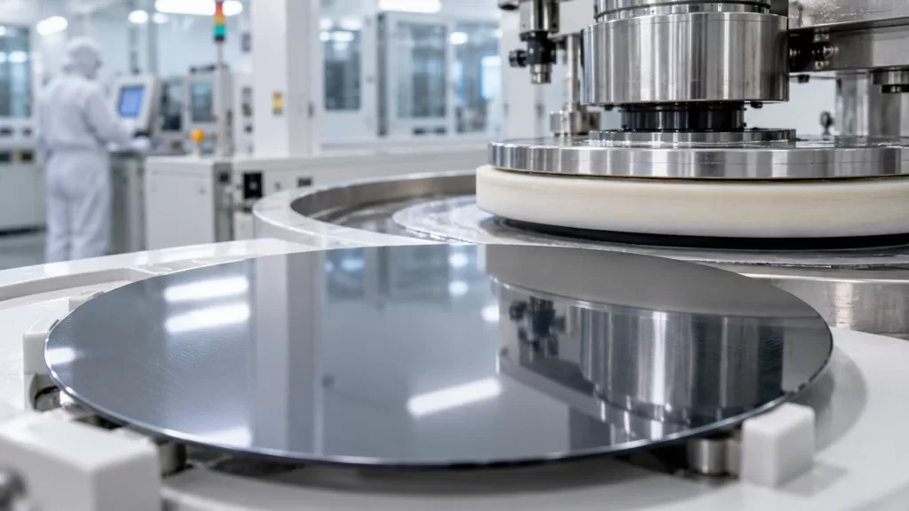
For many years, SiC wafer polishing was evaluated primarily by one number:
surface roughness.
A low Ra value remains essential. Yet the semiconductor industry is increasingly recognizing that a surface can appear extremely smooth while still containing mechanical damage below the surface.
For an epi-ready SiC substrate, this hidden damage can be just as important as the visible surface finish.
Recent 2026 research is therefore focusing not only on achieving sub-nanometer roughness, but also on increasing material removal rate while reducing scratches, micro-pits, lattice damage and subsurface defects.
Why SiC Is Difficult to Polish
4H-SiC has a Mohs hardness close to that of diamond and strong Si-C chemical bonds.
This creates a fundamental processing challenge.
Pure mechanical polishing can remove material relatively quickly, but aggressive abrasive action may introduce scratches, pits and subsurface damage.
Pure chemical reactions, on the other hand, tend to be too slow because the SiC surface is chemically stable.
Chemical mechanical polishing, or CMP, attempts to solve this problem by combining both mechanisms.
The surface is chemically modified into a softer reaction layer, and abrasive particles subsequently remove that layer.
The cycle repeats continuously until a smooth surface is produced.
The challenge is achieving an economically useful removal rate without damaging the crystal underneath.
Surface Roughness Is Only Part of the Specification
A polished SiC wafer may have a surface roughness below one nanometer and still contain residual damage created during slicing, grinding or polishing.
This is referred to as subsurface damage.
It can include lattice distortion, dislocations, microcracks, amorphous regions and vacancy-related defects.
Such defects are particularly important because the polished Si-face is normally used for subsequent homoepitaxial growth.
If the starting surface contains significant residual damage, epitaxial growth may reproduce or amplify some surface irregularities.
For a research wafer, a small local defect may be acceptable.
For volume manufacturing, however, the objective is to provide an entire wafer surface that behaves consistently during epitaxy.
This is why modern wafer qualification increasingly combines atomic-force microscopy and optical inspection with defect characterization methods capable of evaluating damage below the immediate surface.
2026 Research Is Targeting the Removal-Rate Versus Quality Trade-Off
One of the persistent problems in SiC CMP is the trade-off between polishing speed and surface quality.
Hard abrasives can provide high material removal rates but may generate mechanical damage.
Softer abrasives generally reduce scratching but often polish more slowly.
Several studies published in 2026 have attempted to change this relationship.
Research on CeO₂@C₆₀ composite abrasives reported a material removal rate of approximately 334 nm/h while reducing SiC surface roughness to about 0.57 nm. The reported removal rate was around 2.6 times that obtained with conventional CeO₂ abrasives under the study conditions.
Another study evaluated sub-micron Na-Y zeolite particles as SiC CMP abrasives. The researchers reported removal performance comparable with harder alumina abrasives while achieving smoother surfaces, illustrating the growing interest in chemically active “soft” abrasives.
These studies are important because they show where the industry is trying to go:
more chemical assistance and less destructive mechanical force.
Low-Damage Polishing Is Becoming More Important
The polishing target for SiC is no longer simply “make the wafer shiny.”
The objective is to remove the damaged layer left by upstream processes while creating a surface suitable for epitaxy.
A 2026 study on liquid-film shearing polishing of 4H-SiC reported a material removal rate of 6.84 μm/h and surface roughness of approximately 0.37 nm. More importantly, the researchers reported subsurface damage on the order of only about 1 nm under optimized conditions.
The exact values from laboratory studies cannot automatically be transferred to production equipment, but the direction is significant.
Polishing technology is being evaluated simultaneously in terms of:
material removal rate,
surface roughness,
surface-defect density,
and subsurface damage.
For epi-ready wafer manufacturing, all four parameters matter.
Electrochemical and Reactive Polishing Are Expanding
Another direction is electrochemical mechanical polishing.
Instead of depending only on chemical oxidizers in a slurry, an electrochemical reaction is used to modify the SiC surface before mechanical removal.
A 2026 study of cluster-electrode electrochemical mechanical polishing reported that optimized processing reduced 4H-SiC roughness from 16.6 nm to approximately 0.385 nm. The study also investigated radial differences in oxidation behavior and wafer-scale polishing uniformity.
Fenton-reaction-based polishing is also receiving attention.
A September 2026 study using a WS₂-assisted iron-based Fenton slurry reported a material removal rate of 1,168 nm/h together with surface roughness of 0.303 nm for its optimized system.
The practical significance is not that one slurry formulation will immediately become an industry standard.
Rather, the research demonstrates an important trend:
SiC polishing is increasingly being treated as a controlled surface-chemistry problem rather than only an abrasive process.
Why 200 mm Wafers Make CMP More Difficult
Larger SiC wafers create additional polishing challenges.
Maintaining a low roughness value in a small measurement area is relatively straightforward compared with maintaining uniform removal across an entire large-diameter wafer.
In production, CMP must control:
center-to-edge removal rate,
wafer thickness,
total thickness variation,
local flatness,
edge profile,
Bow and Warp.
If the center is polished more rapidly than the edge, thickness uniformity may deteriorate even when local surface roughness appears excellent.
Likewise, aggressive pressure can improve removal rate but may introduce additional deformation or damage.
This is why wafer-scale uniformity becomes increasingly important as SiC moves toward larger substrates.
Research into 8-inch 4H-SiC CMP is already examining new abrasive-size distributions specifically to improve removal efficiency while suppressing surface damage, illustrating how polishing technology is adapting to larger wafer diameters.
Si-Face and C-Face Do Not Polish Identically
A 4H-SiC wafer has two polar surfaces: the silicon-terminated Si-face and the carbon-terminated C-face.
Their chemical reactivity is different.
For most power-device applications, the Si-face is the device and epitaxy surface and therefore requires the highest-quality CMP finish.
The C-face may receive a different polishing specification depending on whether the wafer is single-side polished or double-side polished.
Because oxidation and removal mechanisms differ between the two surfaces, a CMP recipe optimized for one face cannot always be directly applied to the other.
This polarity-dependent behavior is another reason why SiC polishing is fundamentally more complex than simply using progressively smaller abrasive particles.
What an Epi-Ready SiC Surface Should Provide
For semiconductor customers, the final objective is not the polishing process itself.
The objective is a wafer that can enter an epitaxial reactor with minimal additional preparation and deliver stable epitaxial growth.
An epi-ready surface therefore requires more than a low Ra value.
It should provide low scratch density, minimal pits, low residual particles, controlled surface chemistry, low subsurface damage and stable wafer geometry.
Cleaning after CMP is equally important because residual abrasive particles or metallic contamination can affect downstream semiconductor processing.
As power-device manufacturing becomes more demanding, the value of the starting substrate will increasingly depend on how predictable it is during epitaxy.
From “Smooth” to “Process-Ready”
The SiC industry has already made enormous progress in polishing.
Sub-nanometer surface roughness is now achievable using multiple processing approaches.
The next stage is more difficult.
Manufacturers need to achieve that surface quality with high throughput, low consumable cost, minimal damage and excellent wafer-scale uniformity.
This is why polishing research in 2026 is moving beyond the traditional roughness number.
For device manufacturers, a wafer with Ra below 0.2 nm is valuable only when the underlying crystal remains undamaged and the entire surface supports stable epitaxial growth.
The future benchmark for SiC polishing is therefore unlikely to be simply:
“How smooth is the wafer?”
A more meaningful question is:
“How much damage remains underneath that smooth surface, and how consistently can the process deliver an epi-ready wafer?”