Focus on the field of new material !

Silicon dioxide (SiO2) wafers, commonly known as silica wafers, are foundational materials in the semiconductor industry and possess a myriad of applications beyond electronics. This abstract delves into the composition, fabrication processes, structural properties, surface characteristics, and diverse applications of SiO2 wafers, highlighting their significance in modern technology and scientific research.
SiO2 wafers consist primarily of silicon and oxygen atoms arranged in a crystalline lattice structure, with silicon atoms bonded to oxygen atoms in tetrahedral configurations. These wafers are typically manufactured through the thermal oxidation of silicon substrates or via chemical vapor deposition (CVD) techniques, resulting in high-purity, amorphous or crystalline SiO2 films with precise thickness and uniformity.
The structural properties of SiO2 wafers are influenced by factors such as deposition method, temperature, and pressure, leading to variations in film density, refractive index, and mechanical strength. SiO2 films exhibit excellent dielectric properties, thermal stability, and resistance to chemical corrosion, making them ideal for insulating layers, passivation coatings, and protective barriers in semiconductor devices.
Surface characteristics play a crucial role in determining the performance and functionality of SiO2 wafers in various applications. Surface roughness, morphology, and defect density affect film adhesion, optical transparency, and electrical properties, necessitating control and optimization during fabrication processes.
SiO2 wafers find widespread use in the semiconductor industry for fabricating integrated circuits, microelectromechanical systems (MEMS), and nanoelectronic devices. As insulating layers, SiO2 films serve as gate oxides, interlayer dielectrics, and isolation barriers, enabling the miniaturization and integration of semiconductor components.
Beyond electronics, SiO2 wafers have diverse applications in optics, photonics, sensors, and biomedical devices. Their optical transparency, low optical absorption, and biocompatibility make them suitable for optical waveguides, photonic circuits, biosensors, and biomedical implants.
Moreover, SiO2 wafers exhibit potential in emerging fields such as photovoltaics, energy storage, and quantum technologies. Their tunable optical and electronic properties, coupled with scalable manufacturing processes, offer opportunities for innovation and advancement in renewable energy, battery technology, and quantum information science.
In conclusion, SiO2 wafers represent essential materials in semiconductor manufacturing and possess a wide range of applications across various industries and research fields. Their unique combination of structural, surface, and functional properties makes them indispensable for enabling advancements in electronics, optics, energy, and healthcare. As technology continues to evolve, SiO2 wafers are poised to play a pivotal role in shaping the future of modern technology and scientific exploration.
SiO2 silicon dioxide wafers represent a cornerstone material in a wide array of industries, including semiconductor manufacturing, electronics, optics, and biomedical applications, owing to their diverse range of exceptional properties. These properties, including high purity, thermal stability, electrical insulation, optical transparency, chemical inertness, and biocompatibility, render SiO2 wafers indispensable for enabling advancements in technology and scientific research across multiple sectors.
In semiconductor manufacturing, SiO2 wafers play a vital role as insulating layers, gate dielectrics, and passivation coatings in integrated circuits and microelectronic devices. Their high purity and excellent dielectric properties ensure optimal device performance and reliability, while their thermal stability allows for processing at elevated temperatures without degradation.
In electronics, SiO2 wafers are utilized for the fabrication of thin-film transistors, capacitors, and MEMS devices, where their electrical insulation and compatibility with semiconductor materials are crucial for device functionality and performance. Additionally, SiO2 films serve as protective coatings and insulating layers in electronic components and printed circuit boards.
Optical applications benefit from the optical transparency and surface quality of SiO2 wafers, which make them ideal substrates for optical coatings, waveguides, lenses, and mirrors. Their low optical absorption and scattering properties enable efficient transmission of light, facilitating the development of high-performance optical systems and devices for telecommunications, imaging, and sensing applications.
In biomedical fields, SiO2 wafers find applications in biosensors, implantable devices, drug delivery systems, and tissue engineering scaffolds, leveraging their biocompatibility and chemical inertness for safe integration into biological systems. SiO2 materials enable the development of advanced biomedical technologies for diagnostic, therapeutic, and regenerative medicine applications.
As the demand for high-performance materials continues to grow, SiO2 wafers are poised to remain essential components in a wide range of applications across various industries. Ongoing research and development efforts aimed at enhancing the properties and functionalities of SiO2 materials hold promise for unlocking new opportunities and applications in emerging fields such as nanotechnology, quantum computing, renewable energy, and sustainable manufacturing.
In conclusion, SiO2 silicon dioxide wafers stand as versatile and indispensable materials at the forefront of technological innovation, driving progress and advancements in diverse industries and scientific disciplines. Their unique combination of properties and capabilities makes them integral components in the development of cutting-edge technologies and solutions that address complex challenges and pave the way for a brighter and more sustainable future.

SiO2 silicon dioxide wafers serve as foundational materials with versatile applications spanning various industries, including semiconductor manufacturing, electronics, optics, biomedical engineering, environmental monitoring, energy storage, and catalysis. Their remarkable combination of properties, including electrical insulation, optical transparency, biocompatibility, and chemical stability, positions them as indispensable components for driving technological advancements and addressing multifaceted challenges in contemporary society. As research and development endeavors continue to expand, SiO2 wafers are poised to assume a pivotal role in shaping the trajectory of science, technology, and innovation.
In semiconductor manufacturing, SiO2 wafers are instrumental in the production of integrated circuits, microprocessors, and other electronic devices. They serve as insulating layers, gate dielectrics, and passivation coatings, providing electrical insulation and facilitating the miniaturization of semiconductor components. Their high purity and excellent dielectric properties ensure optimal device performance and reliability, while their thermal stability enables processing at elevated temperatures without compromising functionality.
The electronics industry benefits from SiO2 wafers in the fabrication of thin-film transistors, capacitors, and MEMS devices, where their electrical insulation and compatibility with semiconductor materials are critical. Additionally, SiO2 films are utilized as protective coatings and insulating layers in electronic components and printed circuit boards, safeguarding against electrical breakdown and environmental degradation.
Optical applications leverage the optical transparency and surface quality of SiO2 wafers for optical coatings, waveguides, lenses, and mirrors. Their low optical absorption and scattering properties enable efficient transmission of light, enabling the development of high-performance optical systems and devices for telecommunications, imaging, sensing, and spectroscopy.
In biomedical engineering, SiO2 wafers find applications in biosensors, implantable devices, drug delivery systems, and tissue engineering scaffolds, owing to their biocompatibility and chemical inertness. SiO2 materials enable the development of advanced biomedical technologies for diagnostic, therapeutic, and regenerative medicine applications, while their surface properties can be tailored to promote cell adhesion and tissue integration.
Environmental monitoring applications utilize SiO2 wafers for sensor platforms, gas sensors, and environmental monitoring devices. Their stability and compatibility with sensing elements enable accurate detection and analysis of pollutants, gases, and environmental contaminants, contributing to environmental protection and management efforts.
Energy storage technologies benefit from SiO2 wafers in battery systems, supercapacitors, and energy storage devices, where their high surface area and chemical stability enhance electrode performance and cycling stability. SiO2 materials play a role in improving energy storage efficiency, reliability, and safety in renewable energy systems and portable electronics.
Catalysis applications leverage SiO2 wafers as catalyst supports and immobilization matrices for heterogeneous catalysis and enzyme immobilization. Their high surface area, porosity, and thermal stability facilitate catalyst dispersion and enhance catalytic activity and selectivity in chemical reactions, contributing to process efficiency and sustainability.
In conclusion, SiO2 silicon dioxide wafers find multifaceted applications across diverse industries, driving technological innovation and addressing critical societal needs. Their unique properties and versatile capabilities position them as essential components for advancing science, technology, and innovation in the 21st century. As research and development endeavors continue to evolve, SiO2 wafers are poised to remain at the forefront of transformative technologies and solutions that shape the future of society and the global economy.
| Product Name | Silicon Wafer Silicon Dioxide Layer |
| Product Code | NCZ-WM-0015 |
| CAS | 7440-21-3 |
| Diameter | 100 mm, also available in 2, 3, 5, 6, 12″ |
| Type | P/N Type, Undoped |
| Orientation | <100> /other orientations are also available |
| Surface | Single /Both Side Polished |
| Thickness | 400 μm, ask for other wafer thickness |
| Resistivity | 0.01-0.02 Ω-cm |
| SiO2 Thickness Layer | 200 nm (customization available) |

Thermal oxide (silicon dioxide, SiO 2) layer is formed on silicon wafer surface at an elevated temperature in the presence of an oxidant. This process is commonly referred to as a thermal oxidation process.
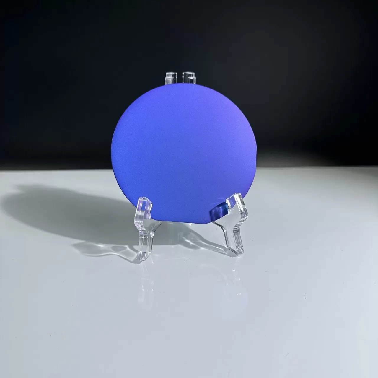
A SiO2 wafer, also known as a silicon dioxide wafer or silica wafer, is a thin slice of silicon dioxide material that is commonly used as a substrate or insulating layer in various semiconductor and electronic devices. Silicon dioxide, or SiO2, is a compound made up of silicon and oxygen atoms arranged in a crystalline or amorphous structure.
SiO2 wafers are typically manufactured through processes such as thermal oxidation of silicon substrates or chemical vapor deposition (CVD) techniques, resulting in high-purity SiO2 films with precise thickness and uniformity. These wafers exhibit properties such as high electrical insulation, thermal stability, optical transparency, and chemical inertness, making them suitable for a wide range of applications in the semiconductor industry, electronics, optics, biomedical engineering, and other fields.
The process of silicon surface passivation by thermal oxidation (silicon dioxide) is critical to the semiconductor industry. It is commonly used to manufacture metal–oxide–semiconductor field-effect transistors (MOSFETs) and silicon integrated circuit chips (with the planar process).