
300mm SiC Wafer Processing After the 12-Inch Breakthrough: Slicing, Grinding, CMP, Edge Exclusion and Yield Challenges
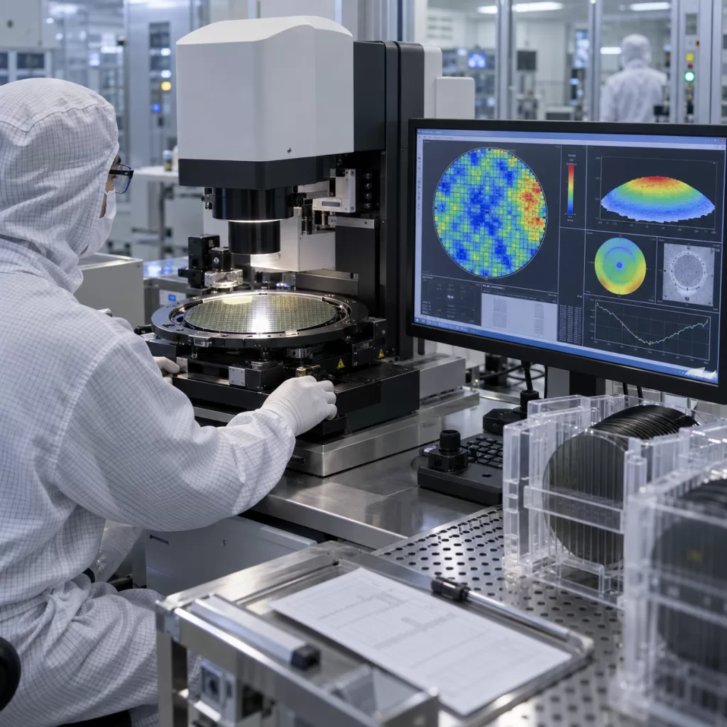
The transition of silicon carbide wafers from 150 mm to 200 mm has already forced the SiC industry to rethink crystal growth, wafer flatness, defect control and equipment compatibility. The emergence of 300 mm, or 12-inch, SiC substrates raises those challenges to an entirely different level. In September 2026, Resonac reported that it had successfully […]
How to Qualify an 8-Inch SiC Wafer Supplier in 2026: Defect Maps, TTV, Bow, Warp, Epi Quality, CoA and Lot Traceability
The transition from 150 mm to 200 mm (8-inch) silicon carbide wafers is changing how semiconductor manufacturers evaluate SiC substrate suppliers. At 150 mm, a buyer may sometimes begin qualification with basic parameters such as diameter, thickness, resistivity, surface roughness and micropipe density. For 200 mm production, that is no longer enough. As wafer diameter […]
300mm High-Thermal-Conductivity SiC Substrates for AI/HPC Packaging: Thermal Conductivity, Flatness, Thickness and Bonding Requirements
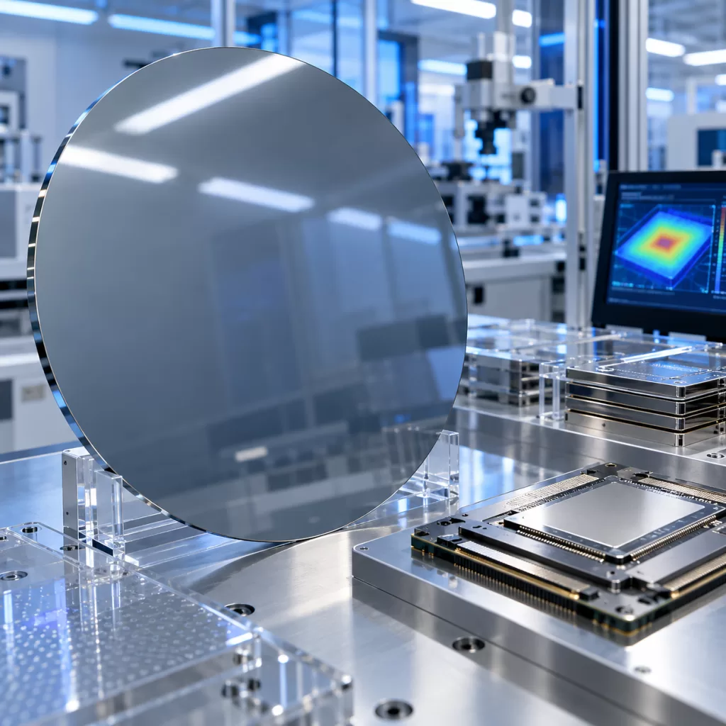
Artificial intelligence accelerators and high-performance computing processors are creating a thermal-management problem that can no longer be solved only by improving external heat sinks or cooling systems. As GPU, accelerator, HBM and chiplet integration becomes denser, a growing portion of the thermal challenge is moving inside the semiconductor package itself. The material directly beneath or […]
Why Advanced SiC Manufacturing Matters: Complexity Drives Technology Leadership
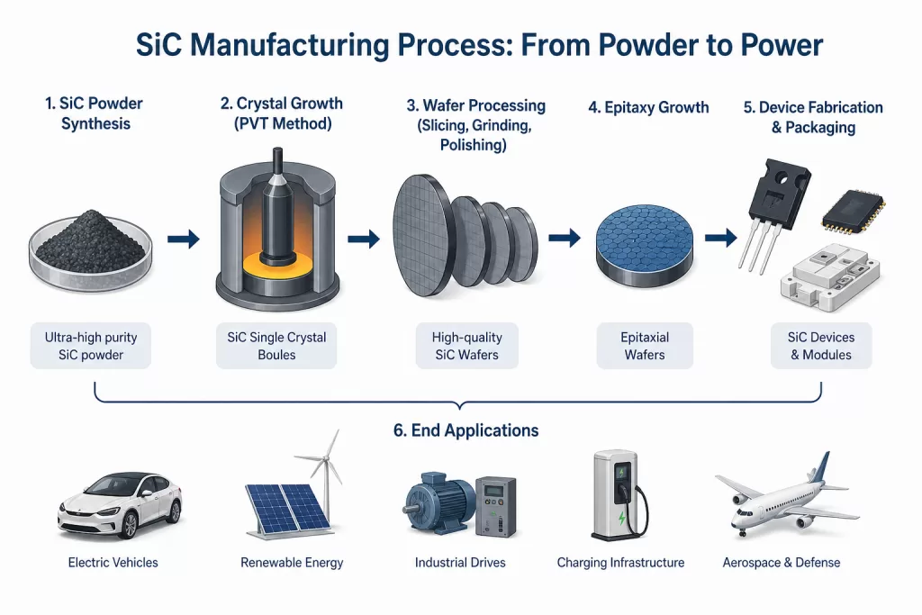
Silicon carbide (SiC) has rapidly become one of the most critical materials in modern semiconductor technology. As industries shift toward high-efficiency power electronics, electric vehicles (EVs), renewable energy systems, and high-frequency devices, the demand for high-quality SiC wafers continues to surge. However, one reality remains clear:the more complex the SiC process, the more critical advanced […]