
The transition of silicon carbide wafers from 150 mm to 200 mm has already forced the SiC industry to rethink crystal growth, wafer flatness, defect control and equipment compatibility. The emergence of 300 mm, or 12-inch, SiC substrates raises those challenges to an entirely different level.
In September 2026, Resonac reported that it had successfully grown and processed a 300 mm SiC single crystal, representing an important milestone in the development of larger-diameter SiC substrates. However, the achievement should not be interpreted as meaning that 300 mm SiC wafers are already available in mature high-volume production. The real challenge begins after crystal growth: converting a large SiC boule into thin, flat, low-damage and epi-ready wafers with acceptable manufacturing yield.
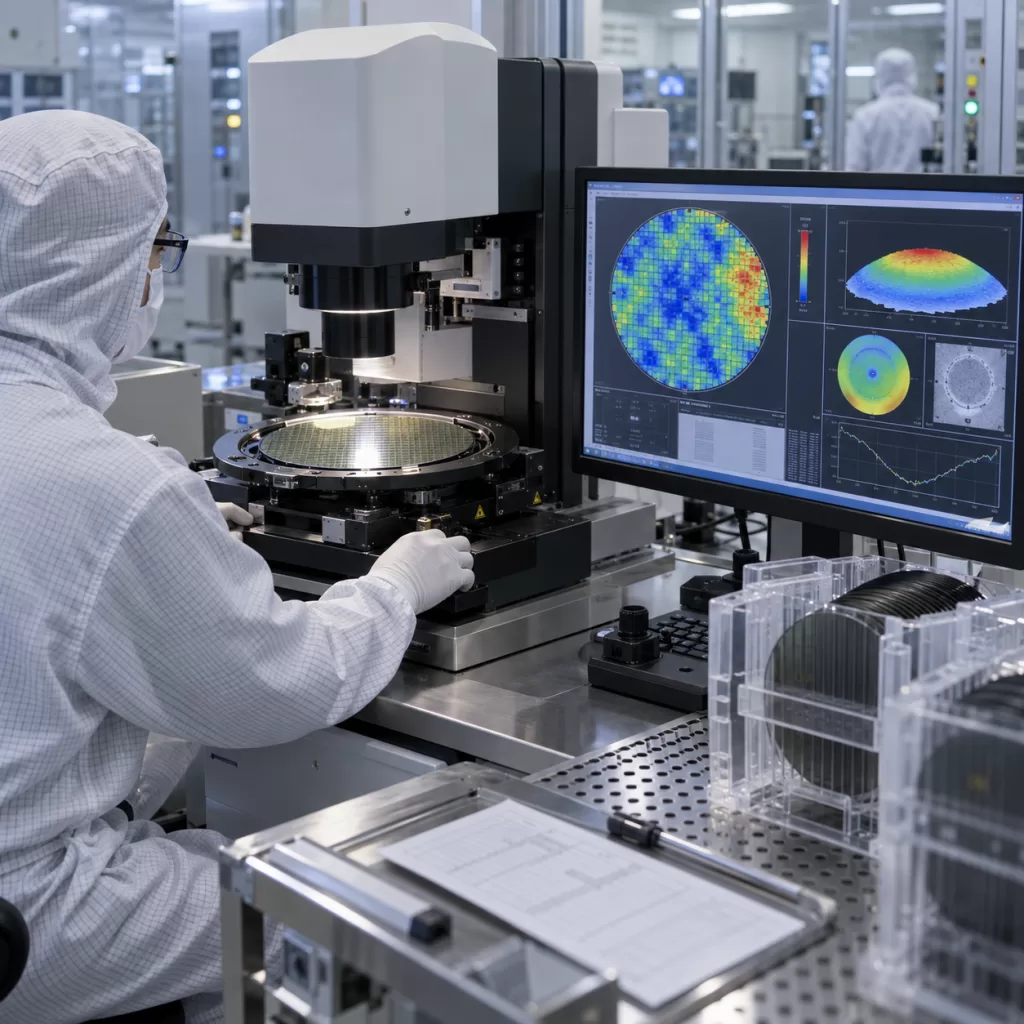
For 300 mm SiC, processes such as slicing, grinding, edge shaping, chemical mechanical polishing (CMP), cleaning and inspection must all be scaled while controlling wafer breakage, subsurface damage, edge defects, TTV, bow, warp and usable-area yield.
This article examines the major wafer-processing challenges that must be solved before 12-inch SiC can move from a technological demonstration toward practical semiconductor manufacturing.
Why Move SiC to 300 mm?
Larger wafer diameters can potentially reduce semiconductor manufacturing cost per device because more chips can be fabricated on each wafer.
A 300 mm wafer has approximately:
- 2.25 times the surface area of a 200 mm wafer
- 4 times the surface area of a 150 mm wafer
In theory, this creates major opportunities for higher fab productivity.
However, wafer economics are not determined by area alone.
If larger SiC wafers introduce higher breakage rates, thicker edge exclusion zones, longer polishing cycles or lower crystal utilization, the theoretical cost advantage can quickly disappear.
This is particularly important for SiC because the material is extremely hard, brittle and expensive to grow. Unlike silicon, SiC wafer manufacturing already requires comparatively intensive slicing, grinding and polishing processes.
Therefore, the central question for 300 mm SiC is not simply:
Can a 300 mm SiC crystal be grown?
It is:
Can that crystal be repeatedly converted into semiconductor-grade wafers at an economically acceptable yield?
1. Slicing a 300mm SiC Boule
Slicing is one of the first major yield-sensitive steps after crystal growth.
Industrial SiC wafer production commonly relies on diamond-wire-based slicing technologies. The objective is to obtain as many wafers as possible from each boule while minimizing:
- kerf loss,
- wafer thickness variation,
- saw marks,
- microcracks,
- residual stress,
- subsurface damage,
- wafer breakage.
Recent research continues to identify slicing loss and mechanically induced damage as important limitations in SiC wafer manufacturing. Conventional wire-based slicing can consume a meaningful portion of the valuable crystal and leave a damaged surface that must later be removed by grinding and polishing.
Why 300mm makes slicing more difficult
As diameter increases, several effects become more important.
First, maintaining a consistent cutting condition across a 300 mm diameter becomes more difficult.
Small variations in wire tension, vibration, abrasive distribution or thermal conditions can translate into larger wafer-level thickness and shape errors.
Second, the larger wafer has greater mechanical leverage during handling. A local crack that might remain harmless on a smaller wafer can propagate during unloading, grinding or cleaning.
Third, the economic value of every 300 mm slice is high. A single broken wafer represents not only material loss but also the loss of all previous crystal-growth and slicing cost.
For this reason, future 300 mm SiC slicing systems will need increasingly precise control of:
- wire tension,
- feed rate,
- cutting speed,
- boule orientation,
- thermal stability,
- vibration,
- coolant or slurry conditions,
- post-slicing wafer handling.
2. Can Laser Slicing Reduce SiC Material Loss?
Laser-assisted and laser-based slicing are attracting growing attention because they may reduce kerf loss compared with conventional mechanical cutting.
A 2026 study on laser-sliced SiC wafers highlighted the potential for substantially lower material loss, but also showed that the laser-modified region creates its own downstream processing challenges. The altered layer can influence grinding behavior and surface integrity and therefore must be carefully removed or controlled.
This illustrates an important principle for next-generation SiC processing:
Reducing loss in one process step cannot come at the expense of dramatically increasing difficulty in the next step.
A slicing method should therefore be evaluated as part of the complete wafer manufacturing chain:
Crystal → Slicing → Grinding → Edge Processing → CMP → Cleaning → Inspection → Epitaxy
For 300 mm wafers, total process yield matters more than the efficiency of any individual step.
3. Grinding: Removing Damage Without Creating New Problems
After slicing, SiC wafers normally require mechanical planarization to remove saw marks, thickness variation and damaged material.
Grinding is particularly challenging because SiC combines:
- very high hardness,
- high elastic modulus,
- chemical stability,
- brittle fracture behavior.
Aggressive grinding can improve throughput, but excessive mechanical loading may introduce:
- microcracks,
- pits,
- scratches,
- residual stress,
- edge chipping,
- deeper subsurface damage.
Very conservative grinding, on the other hand, increases processing time and manufacturing cost.
The challenge is therefore to maximize material removal rate while keeping damage shallow enough for subsequent polishing to remove efficiently.
For 300mm wafers, uniformity becomes critical
A grinding process cannot be optimized only for average wafer thickness.
Manufacturers must simultaneously control:
- total thickness variation (TTV),
- global wafer shape,
- local flatness,
- front-to-back parallelism,
- center-to-edge thickness variation,
- edge profile.
A wafer can meet nominal thickness requirements while still creating problems during epitaxy, lithography or device processing because of excessive local shape variation.
4. CMP Becomes a Major Bottleneck
Chemical mechanical polishing is one of the most important finishing steps for semiconductor-grade SiC wafers.
The goal is to remove remaining mechanical damage and produce an extremely smooth surface suitable for subsequent epitaxial growth.
SiC CMP is more difficult than conventional silicon polishing because SiC is both mechanically hard and chemically resistant.
The process typically depends on a controlled interaction among:
- surface oxidation or chemical modification,
- slurry chemistry,
- abrasive particles,
- polishing pad properties,
- pressure,
- platen speed,
- slurry flow,
- temperature.
As the wafer diameter increases to 300 mm, uniform CMP becomes increasingly difficult.
Center-to-edge uniformity
The polishing rate must remain stable across a much larger surface.
If pressure distribution is not uniform, the wafer may develop:
- excessive center removal,
- excessive edge removal,
- edge roll-off,
- local thickness variation,
- non-uniform surface roughness.
Even relatively small non-uniformities can become significant when propagated through later epitaxy and device fabrication.
CMP throughput
SiC is slow to polish compared with many conventional semiconductor materials.
For 300 mm wafers, simply increasing polishing time is unlikely to be economically attractive.
Future 12-inch production will therefore require improvements in both:
Material removal rate
and
Final surface quality
without trading one for the other.
5. Surface Roughness Is Not the Only CMP Requirement
It is tempting to judge polished SiC primarily by surface roughness.
However, a very low Ra value does not automatically mean the wafer is ready for high-quality epitaxy.
Inspection may also need to evaluate:
- residual scratches,
- polishing pits,
- contamination,
- sub-surface damage,
- local waviness,
- crystal defects exposed during polishing,
- edge damage,
- particles.
For epi-ready SiC substrates, microscopic localized defects can become nucleation points for epitaxial defects or device yield loss.
Therefore, the 300 mm transition will require more comprehensive surface characterization rather than reliance on a single roughness specification.
6. Edge Exclusion Becomes More Economically Important
Wafer edges are particularly difficult regions to process.
During slicing, grinding, edge shaping, polishing and handling, the outer region is exposed to different mechanical and polishing conditions than the wafer center.
Potential defects include:
- edge chips,
- microcracks,
- bevel scratches,
- polishing roll-off,
- particle accumulation,
- local thickness variation.
Semiconductor fabs therefore define an edge exclusion region where device fabrication or critical metrology may not be considered valid.
For expensive 300 mm SiC substrates, this dimension has direct economic consequences.
A larger edge exclusion means a smaller usable wafer area.
When scaling from 150 or 200 mm to 300 mm, wafer suppliers should therefore focus not only on nominal diameter but also on the effective usable diameter after edge exclusion.
Important RFQ parameters may include:
| Parameter | Why It Matters |
|---|---|
| Wafer diameter | Equipment compatibility |
| Edge exclusion | Determines usable processing area |
| Edge profile | Influences chipping and mechanical strength |
| Edge polishing | Helps control particles and edge defects |
| TTV | Affects process uniformity |
| Bow | Indicates global curvature |
| Warp | Indicates overall wafer distortion |
| Surface roughness | Critical for epitaxy and bonding |
| Front-side defects | Influences epi and device yield |
| Backside condition | Affects chucking and handling |
7. Bow, Warp and TTV Become Harder to Control at 300mm
Wafer geometry becomes increasingly important as diameter increases.
Three common parameters are:
TTV — Total Thickness Variation
TTV describes the difference between the maximum and minimum measured wafer thickness.
High TTV may lead to non-uniform contact, polishing, lithography or epitaxy.
Bow
Bow represents the deviation of the wafer’s median surface from a reference plane when the wafer is in an unconstrained condition.
Warp
Warp describes the difference between the maximum and minimum deviations of the wafer’s median surface from a reference plane.
Although these parameters are already important for 150 mm and 200 mm SiC, controlling them across a 300 mm wafer requires more uniform:
- slicing,
- grinding,
- polishing,
- thermal treatment,
- material stress.
The larger area means small local processing differences can produce significant wafer-level geometry changes.
8. Handling and Automation Become Part of Wafer Quality
At 300 mm, manual handling becomes increasingly undesirable.
Automated wafer handling must minimize:
- backside scratches,
- edge contact,
- particle contamination,
- mechanical shock,
- vacuum-induced stress.
Robots, wafer carriers, cassettes and inspection equipment must also be compatible with the wafer’s thickness, stiffness and edge geometry.
This creates an additional challenge during early 300 mm SiC development: wafer manufacturing technology and downstream semiconductor equipment must evolve together.
A high-quality substrate is of limited value if available equipment cannot safely transport, measure or process it.
9. The Real Metric Is Cumulative Yield
For large-diameter SiC, yield should not be considered only at the crystal-growth stage.
A simplified wafer manufacturing yield chain may look like:
Boule yield × slicing yield × grinding yield × polishing yield × inspection yield = final wafer yield
For example, even if every individual process achieves a relatively high yield, accumulated losses across multiple steps can become economically significant.
As diameter increases, manufacturers will therefore need tighter statistical process control throughout the entire production chain.
Key process indicators may include:
- wafers obtained per boule,
- kerf loss,
- slicing breakage rate,
- grinding removal amount,
- post-grinding damage depth,
- CMP removal rate,
- surface defect density,
- edge defect rate,
- wafer geometry distribution,
- final epi-ready yield.
This is why the 300 mm SiC transition is fundamentally a manufacturing integration challenge, not simply a crystal-size challenge.
10. What Does the 12-Inch Breakthrough Mean for the SiC Industry?
The successful demonstration of grown and processed 300 mm SiC crystals is significant because it confirms that the industry is already looking beyond the current 150 mm and 200 mm production landscape.
However, history from previous semiconductor wafer-size transitions shows that increasing diameter does not automatically produce lower-cost wafers.
Large-diameter wafer economics depend on achieving sufficient:
- process yield,
- throughput,
- equipment utilization,
- defect control,
- metrology capability,
- standardization.
For SiC, these challenges are amplified by the material’s hardness, brittleness and relatively high crystal value.
The next important milestones will therefore be less about whether another 300 mm crystal can be produced and more about whether manufacturers can repeatedly demonstrate:
- stable 300 mm crystal quality,
- high slicing yield,
- low wafer breakage,
- controlled TTV, bow and warp,
- uniform CMP,
- narrow edge exclusion,
- epi-ready surface quality,
- repeatable lot-to-lot specifications,
- acceptable cost per usable wafer area.
What Buyers Should Ask About Future 300mm SiC Wafers
For R&D programs evaluating large-diameter SiC substrates, a quotation should eventually specify more than diameter and thickness.
A useful technical inquiry should include:
Crystal
- Polytype: 4H-SiC
- Conductivity type: N-type, semi-insulating or other
- Orientation
- Off-axis angle
- Resistivity
Dimensions
- Diameter
- Thickness
- Thickness tolerance
- TTV
- Bow
- Warp
Surface
- Si-face or C-face polishing
- Single-side or double-side polished
- Surface roughness
- Scratch/pit criteria
- Particle specification
Edge
- Edge profile
- Edge exclusion
- Edge polishing
- Chip specification
Defects
- Micropipe density
- BPD/TSD/TED criteria where applicable
- Surface defect map
- Inspection method
Documentation
- Certificate of Analysis
- Wafer map
- Lot traceability
- Inspection report
- Packing method
These parameters become increasingly important as SiC wafers move from research samples toward production-qualified substrates.
Conclusion
The development of 300 mm SiC is an important technological milestone, but crystal diameter alone does not determine whether 12-inch SiC can become commercially successful.
The decisive challenge lies in wafer processing.
Slicing must minimize material loss and damage. Grinding must achieve thickness and shape control without generating deep defects. CMP must deliver uniform epi-ready surfaces across a much larger area. Edge processing must protect mechanical strength while keeping edge exclusion small. Automated handling and metrology must support the larger format without introducing additional damage.
Ultimately, 300 mm SiC will succeed only when the industry can combine large diameter, high crystal quality, tight wafer geometry and acceptable cumulative manufacturing yield.
The transition from 200 mm to 300 mm therefore represents much more than another increase in wafer diameter.
It represents the next major test of whether SiC manufacturing can achieve the process control and cost efficiency required for the next generation of power electronics and high-volume semiconductor applications.
FAQ
Is 300mm SiC already in mass production?
No. Publicly reported 300 mm SiC developments represent important R&D and manufacturing milestones, but they should not be confused with mature high-volume commercial production. Further improvements in crystal quality, wafer processing, equipment compatibility and manufacturing yield are still required.
Why is SiC wafer slicing more difficult than silicon wafer slicing?
SiC is significantly harder and more brittle than silicon. Slicing therefore requires diamond-based processing and careful control of kerf loss, microcracks, saw damage, wafer thickness variation and mechanical stress. These challenges become more significant as wafer diameter increases.
Why is CMP important for 300mm SiC wafers?
CMP removes residual grinding damage and creates the ultra-smooth surface required for high-quality SiC epitaxy. At 300 mm, maintaining consistent removal rate, surface roughness and center-to-edge uniformity across the entire wafer becomes substantially more difficult.