
Laser Stealth Dicing of SiC Wafers: Subsurface Microcracks, Edge Chipping, Dicing Quality, Inspection and Yield Control
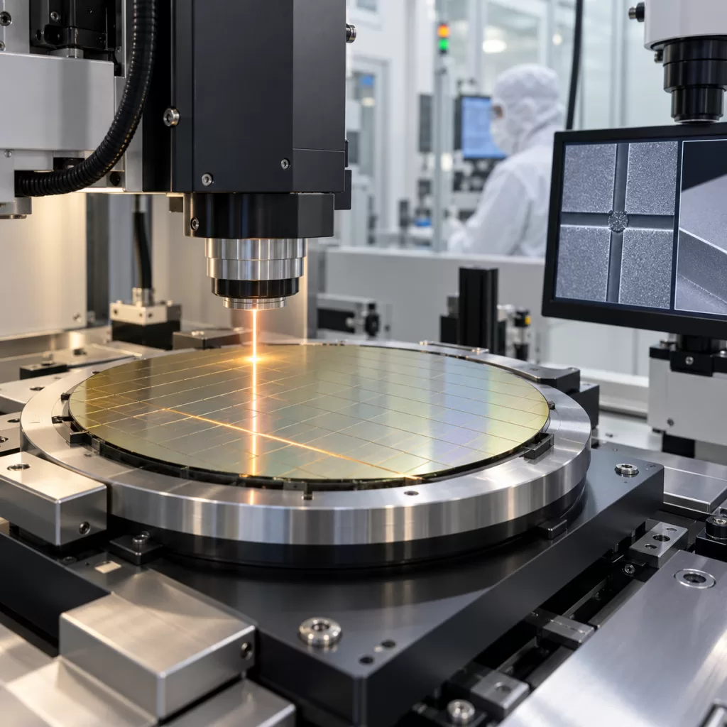
Silicon carbide wafers are increasingly used in high-power and high-temperature semiconductor devices, but they also present major challenges during singulation. Because SiC is extremely hard and brittle, conventional blade dicing can cause edge chipping, kerf loss, mechanical stress and tool wear. As device structures become smaller and wafer value increases, manufacturers are paying more attention […]
Thin SiC Wafer Handling from Backgrinding to Dicing: Ring Frame Mounting, Tape Stress, Warpage and Edge Chipping Control
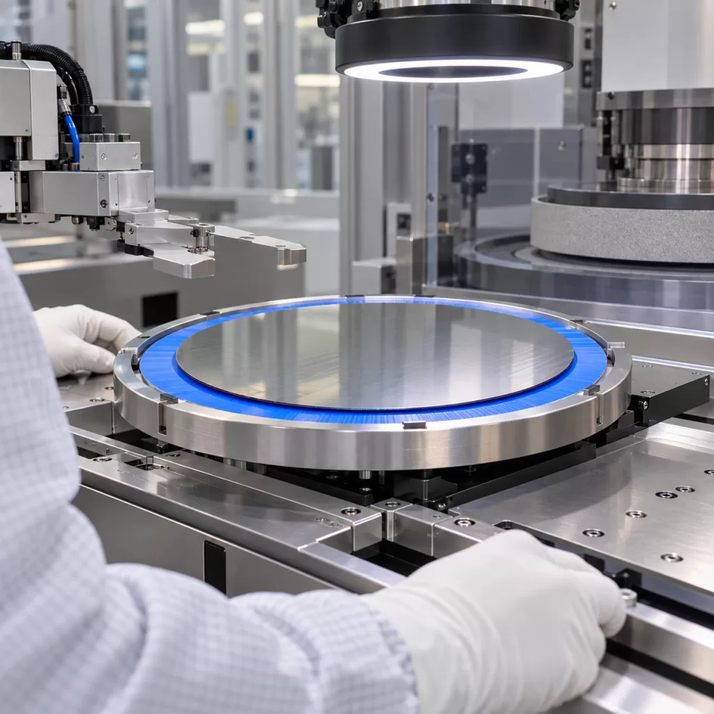
As silicon carbide wafers move toward thinner substrates for power semiconductor manufacturing, wafer handling becomes increasingly important. A standard SiC wafer may remain relatively rigid during conventional processing, but after backgrinding, the reduction in thickness significantly increases sensitivity to bending stress, local pressure, tape tension and mechanical impact. For thin SiC wafers, the transition from […]
SiC Wafer Backgrinding and Thin-Wafer Handling Guide: Thickness Control, Chipping, Warpage and Temporary Carriers
As silicon carbide devices move toward higher power density, thinner packages, and more advanced integration, wafer thinning has become an increasingly important step in SiC device manufacturing. Compared with conventional silicon, silicon carbide is significantly harder and more brittle. These properties make SiC attractive for high-power and high-temperature applications, but they also create additional challenges […]