News
Custom SiC Wafer Solutions: From Sizes to Doping
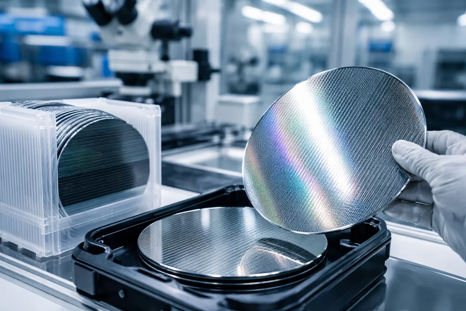
SiC wafer have become a foundational material in modern power electronics and high-frequency devices, driven by their superior physical and electrical properties. Compared with conventional

SiC wafer have become a foundational material in modern power electronics and high-frequency devices, driven by their superior physical and electrical properties. Compared with conventional
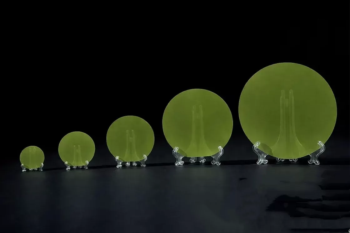
Silicon carbide (SiC), a third-generation semiconductor material, has attracted significant attention due to its wide bandgap, high breakdown electric field, and superior thermal conductivity. These
As industrial automation continues to advance, the demand for high-performance equipment in manufacturing, logistics, and smart production lines has grown significantly. Such systems require precise
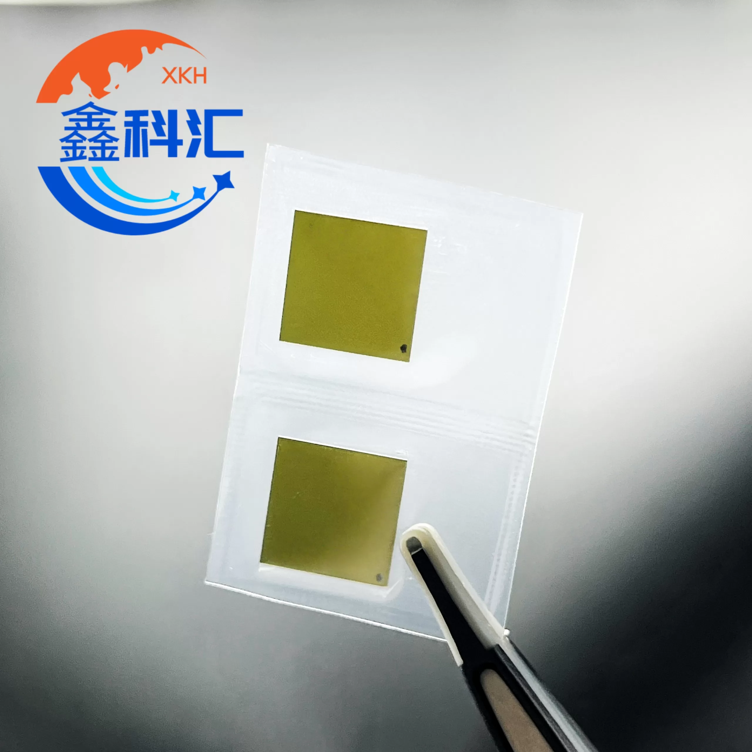
Silicon carbide (SiC) wafers have rapidly gained attention in high-frequency and high-power electronics due to their superior material properties compared to conventional silicon (Si). With
Silicon Carbide (SiC) is rapidly gaining attention in the field of high-temperature electronics due to its superior physical, thermal, and electrical properties compared to traditional
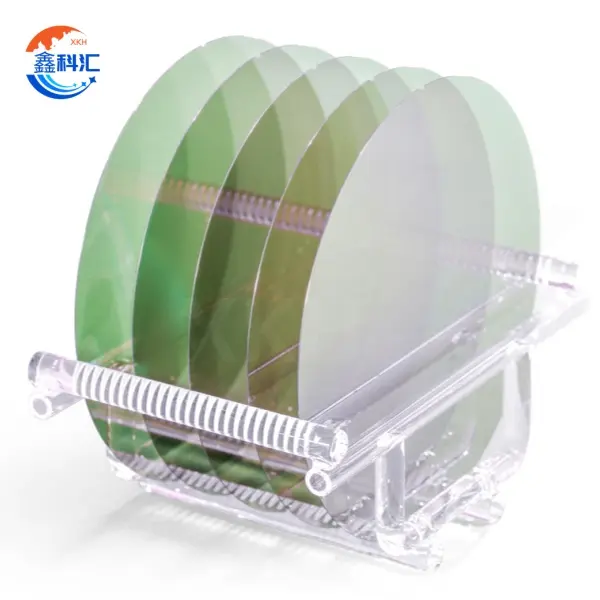
1. Introduction: From Wafer Diameter to Industrial Capability In semiconductor technology, wafer diameter has historically served as a reliable indicator of manufacturing maturity. Each major
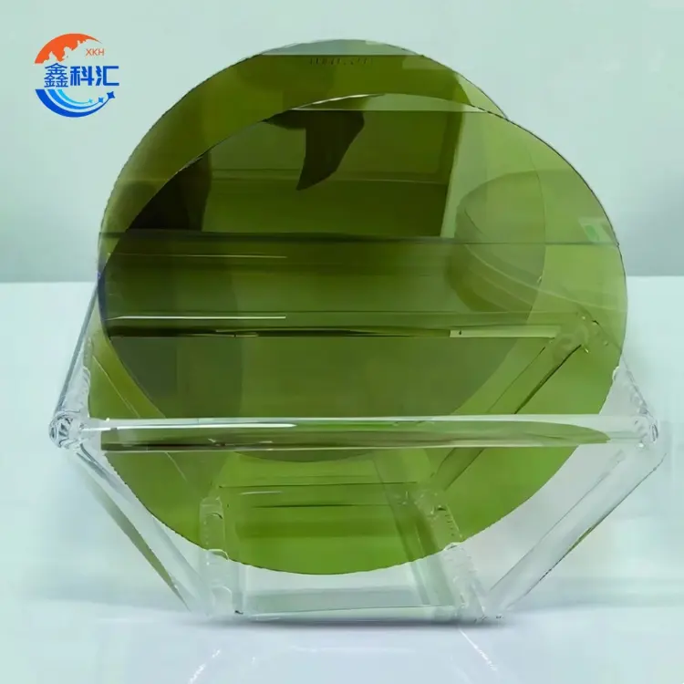
Silicon Carbide (SiC) stands today as one of the most strategically important materials in advanced manufacturing and power electronics. It is widely used in electric

Silicon carbide (SiC) has rapidly moved from a niche material known only to semiconductor experts to a headline technology powering electric vehicles, renewable energy systems,