
Açıklama
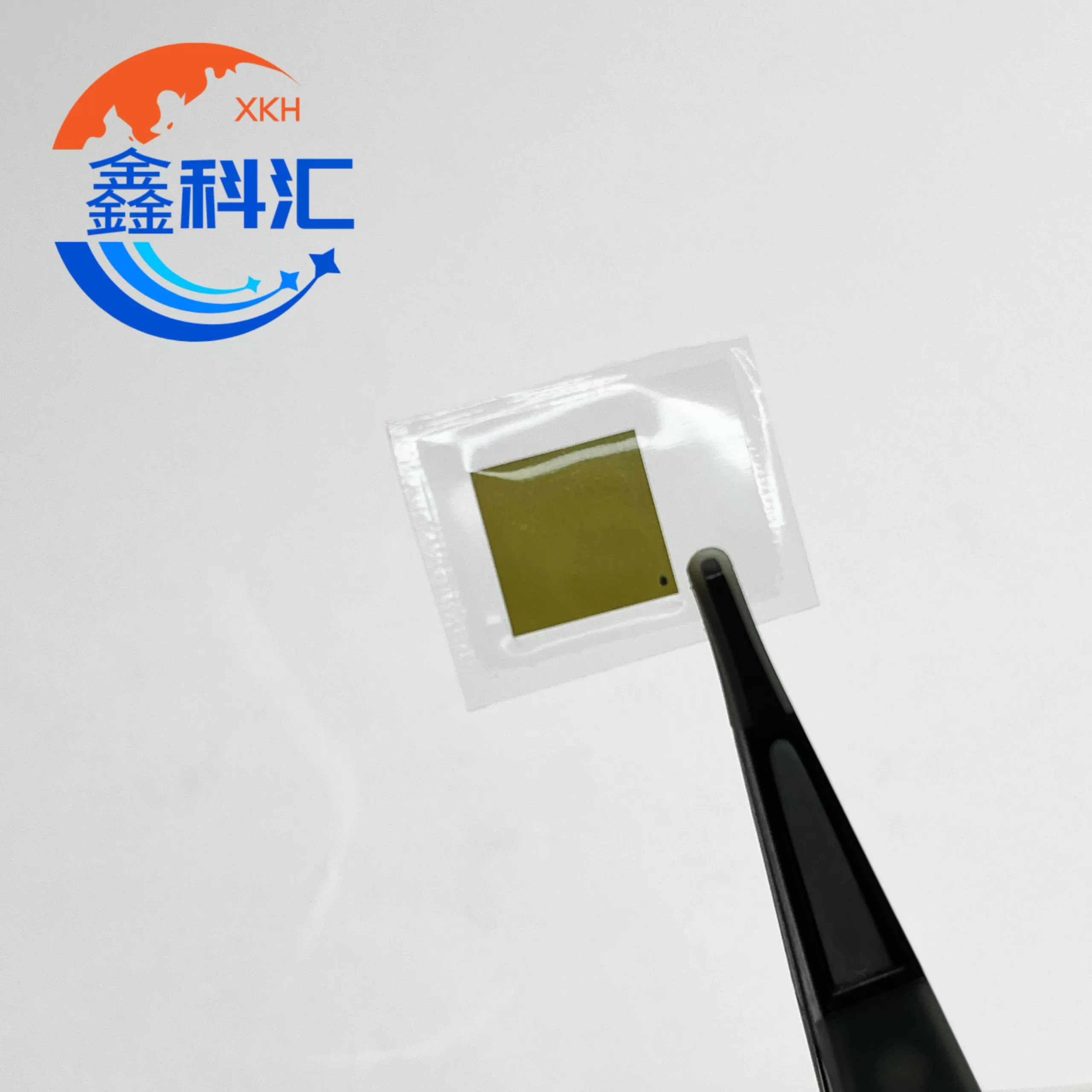
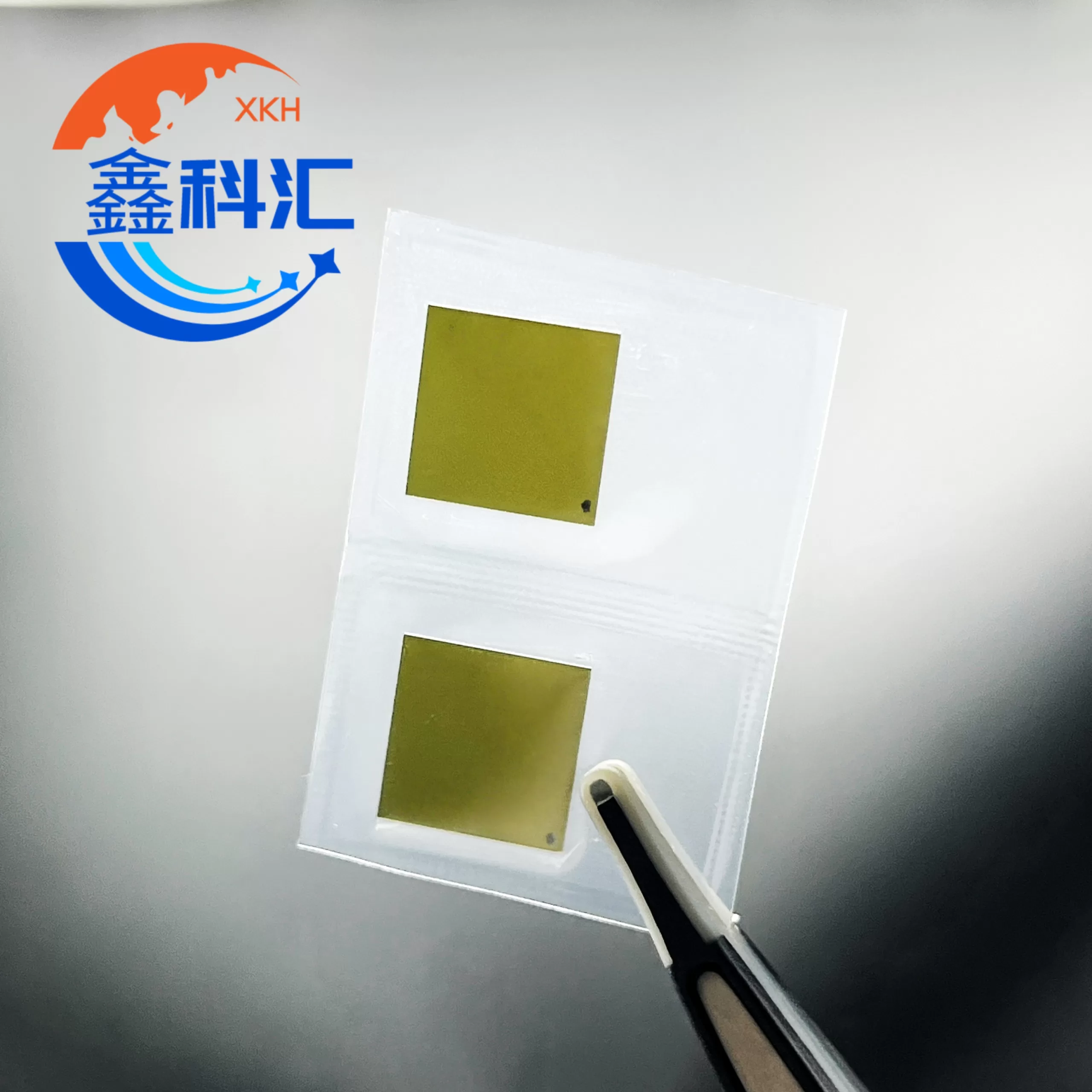
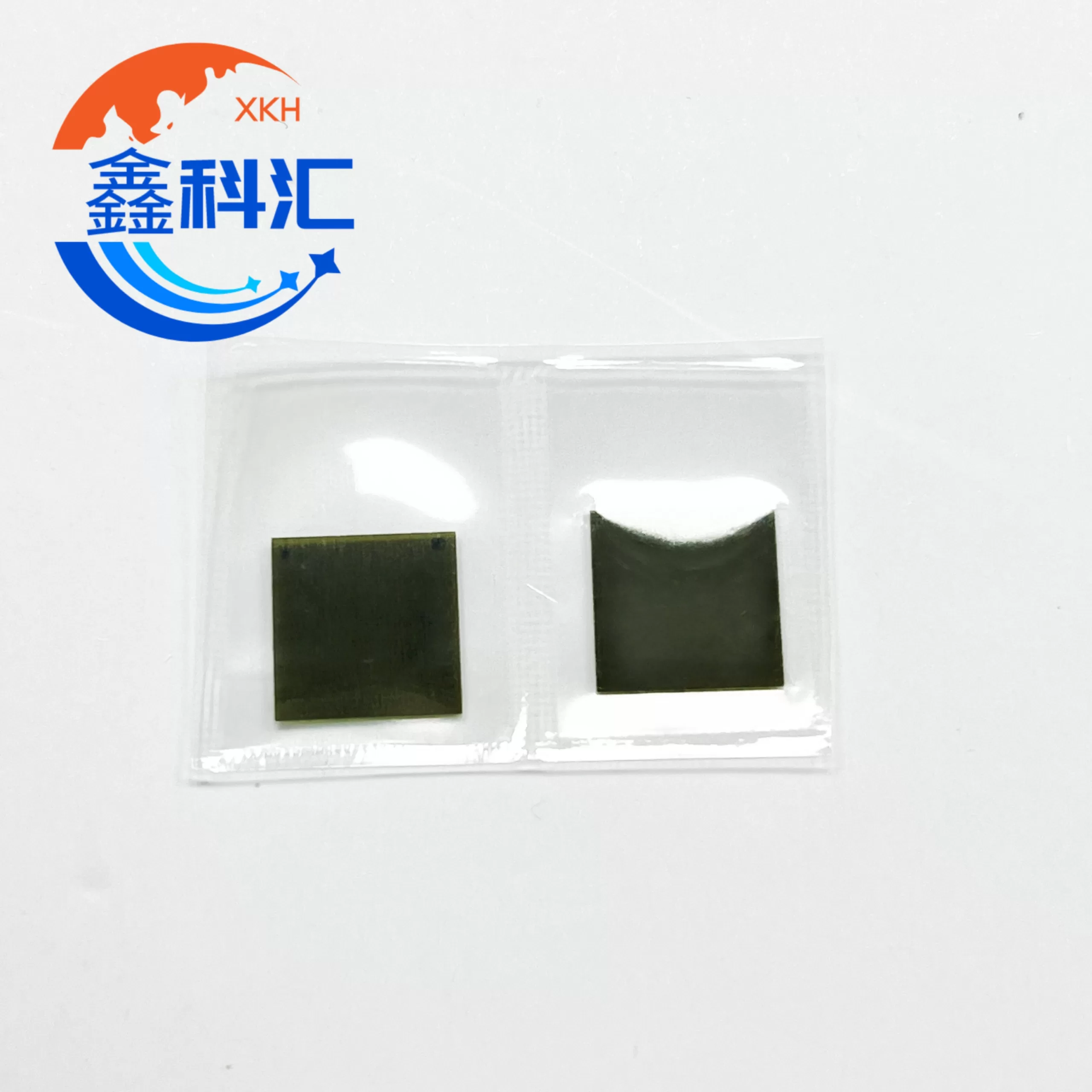
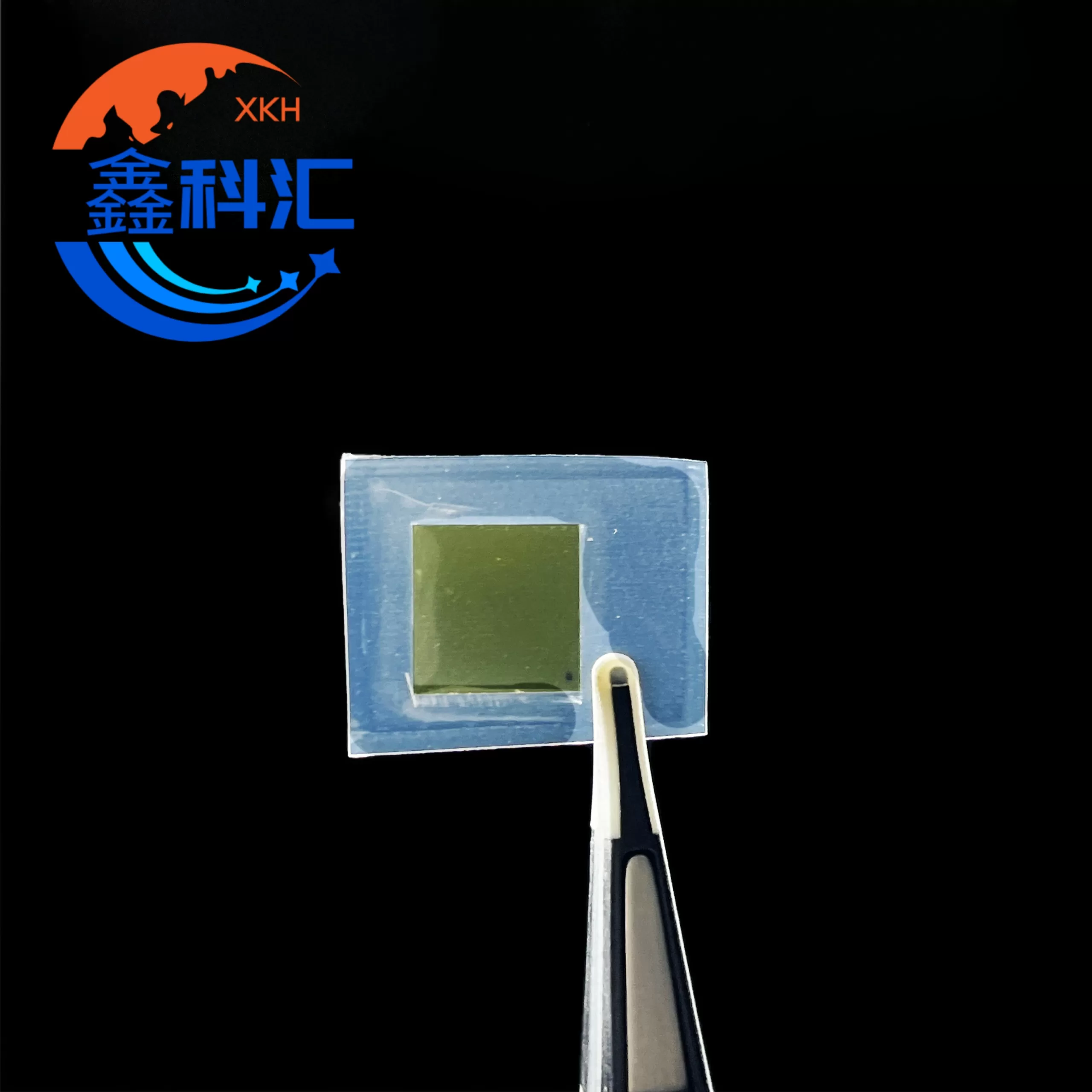
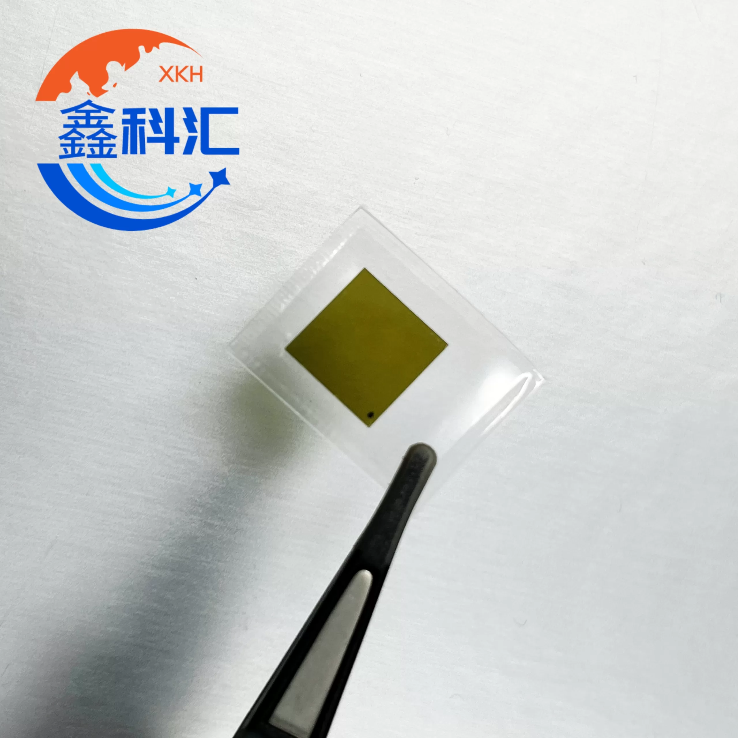
The 4H-N SiC Substrate is a high-purity, single-crystal semiconductor material manufactured using the Physical Vapor Transport (PVT) method. With extremely low defect density, excellent thermal conductivity, and stable electrical characteristics, it is widely used in power electronics, RF/microwave components, and UV optoelectronic devices.
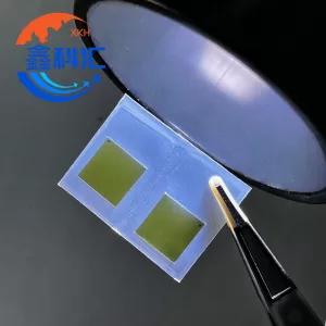
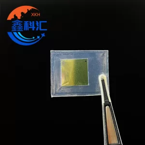
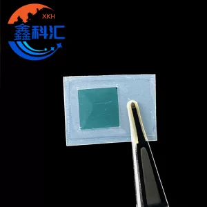
The compact 10×10 mm format is ideal for R&D, device prototyping, epitaxial testing, and laboratory semiconductor research.
Temel Özellikler
Prime-Grade Crystal Quality
Polytype: 4H-SiC
Conductivity: N-type
Micropipe Density (MPD): <1 cm⁻²
Threading Dislocation Density: <10⁴ cm⁻²
Ultra-Smooth, Epi-Ready Surfaces
Si-face (CMP): Ra ≤ 0.5 nm
C-face: Ra ≤ 1 nm
Suitable for MOCVD, CVD, and HVPE epitaxy
Stable Electrical Properties
Resistivity: 0.01–0.1 Ω·cm
Carrier concentration: 1×10¹⁸ – 5×10¹⁹ cm⁻³
Supports high-voltage and high-frequency device structures
Excellent Thermal Performance
Thermal conductivity: ~490 W/m·K
Operating temperature: up to 600°C
CTE: 4.0×10⁻⁶ /K
High Mechanical Strength
Vickers hardness: 28–32 GPa
Flexural strength: >400 MPa
Highly durable and wear-resistant
Teknik Özellikler
| Category | Şartname |
|---|---|
| Malzeme | 4H-SiC Single Crystal (N-type) |
| Dimensions | 10×10 mm (±0.05 mm) |
| Thickness Options | 100–500 μm |
| Oryantasyon | (0001) ± 0.5° |
| Yüzey Kalitesi | CMP / Polished, Ra ≤ 0.5 nm |
| Dirençlilik | 0.01–0.1 Ω·cm |
| Termal İletkenlik | 490 W/m·K |
| Defects | MPD < 1 cm⁻² |
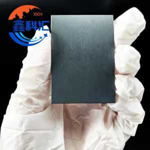
| Renk | Green-tea surface tone |
| Grade Options | Prime, Research, Dummy |
Available Customization
Sizes: 5×5 mm, 5×10 mm, 10×20 mm, Ø2–8 inch
Thickness: 100–500 μm or custom
Orientation: on-axis, 4°, or 8° off-axis
Surface Finish: SSP/DSP optional
Doping Options: N-type, P-type, semi-insulating
Backside metallization available
Uygulamalar
Güç Elektroniği
SiC MOSFETs, Schottky diodes, high-voltage power devices.
RF & 5G Communication
RF power amplifiers, mm-wave modules, high-frequency switches.
New Energy Vehicles
EV inverters, power module development, wide-bandgap testing.
Havacılık ve Savunma
High-temperature, radiation-resistant device manufacturing.
Optoelectronics
UV LEDs, photodiodes, GaN/AlN epitaxy, laser structures.
Research & Laboratory Use
Material characterization, epitaxy research, device prototyping.
SSS
1. What advantages does 4H-SiC have over 6H-SiC?
4H-SiC provides higher electron mobility, lower on-resistance, and better performance in high-power and high-frequency devices.
2. Do you supply conductive or semi-insulating SiC substrates?
Yes. Both N-type conductive and semi-insulating 4H-SiC substrates are available with customizable resistivity.
3. Is this substrate ready for epitaxy?
Yes. The CMP-polished Si-face is epi-ready and suitable for GaN, AlN, and SiC epitaxial growth using MOCVD, CVD, or HVPE.


Değerlendirmeler
Henüz değerlendirme yapılmadı.