
1. Introduction
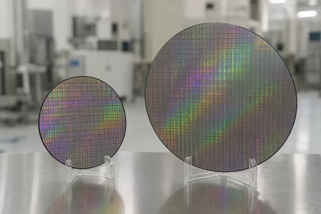
In modern semiconductor manufacturing, wafer size plays a critical role in determining production efficiency, device performance, and overall cost structure. Among the most widely used wafer formats, 200mm (8-inch) and 300mm (12-inch) wafers represent two major generations of fabrication technology.
While 200mm wafers remain essential in legacy and specialized applications, 300mm wafers dominate advanced semiconductor production due to their superior scalability and economic advantages.
This article provides a comprehensive comparison of 300mm and 200mm wafers, focusing on their physical characteristics, manufacturing implications, and practical use cases.
2. Basic Definitions and Dimensions
Semiconductor wafers are thin slices of crystalline material—typically silicon or silicon carbide—used as substrates for device fabrication.
Standard Wafer Dimensions
| Parameter | 200mm Wafer (8-inch) | 300mm Wafer (12-inch) |
|---|---|---|
| Diameter | 200 mm | 300 mm |
| Radius | 100 mm | 150 mm |
| Surface Area | ~31,400 mm² | ~70,700 mm² |
| Typical Thickness | ~725 µm | ~775 µm |
| Edge Type | Notch / Flat | Notch only |
👉 A 300mm wafer has over 2.25 times the surface area of a 200mm wafer, significantly increasing the number of chips that can be fabricated per wafer.
3. Mathematical Relationship of Wafer Area
A=πr2A = \pi r^2A=πr2
The wafer area is calculated using the standard circle area formula. Since the radius increases from 100 mm (200mm wafer) to 150 mm (300mm wafer), the total usable area increases nonlinearly.
This geometric scaling is the foundation of the economic advantage of larger wafers.
4. Key Differences Between 300mm and 200mm Wafers
4.1 Production Efficiency
- 300mm wafers enable significantly higher chip output per fabrication cycle
- Reduced cost per die due to economies of scale
- More efficient utilization of expensive lithography and deposition equipment
In contrast:
- 200mm wafers produce fewer chips per batch
- Higher cost per chip in high-volume production
4.2 Equipment and Infrastructure
300mm wafer fabrication requires:
- Fully automated handling systems (FOUP-based)
- Advanced lithography tools compatible with larger substrates
- Higher capital investment
200mm wafer fabs:
- Often semi-automated or manually assisted
- Lower equipment cost
- Widely available in mature fabs
4.3 Technology Node Compatibility
| Wafer Size | Typical Technology Nodes |
|---|---|
| 200mm | 90nm – 350nm (mature nodes) |
| 300mm | 5nm – 65nm (advanced nodes) |
- 300mm wafers are used in cutting-edge logic, memory, and high-performance computing
- 200mm wafers dominate in analog, power devices, MEMS, and sensors
4.4 Yield and Defect Density
- Larger wafers introduce challenges in uniformity and defect control
- However, modern fabs have optimized 300mm processes to maintain high yields
200mm wafers:
- More stable and mature processes
- Lower risk for small-batch or specialized production
4.5 Cost Structure
Although 300mm fabs require higher initial investment:
- Lower cost per chip in high-volume production
- Better long-term ROI for large-scale manufacturing
200mm fabs:
- Lower entry cost
- Ideal for low-to-medium volume production
5. Application Differences
5.1 300mm Wafer Applications
300mm wafers are widely used in:
- Advanced CPUs and GPUs
- DRAM and NAND memory
- AI chips and high-performance processors
- Advanced CMOS technologies
These applications demand:
- High integration density
- Advanced lithography (EUV)
- Large-scale production
5.2 200mm Wafer Applications
200mm wafers remain highly relevant in:
- Power electronics (IGBT, MOSFET)
- MEMS devices (sensors, actuators)
- Analog ICs
- Automotive electronics
- RF devices
These sectors prioritize:
- Reliability
- Cost efficiency
- Long product lifecycle
6. Industry Trends and Transition
The semiconductor industry has largely transitioned to 300mm wafers for advanced nodes. However, 200mm wafers continue to experience strong demand due to:
- Automotive electronics growth
- IoT expansion
- Power semiconductor applications
Interestingly, capacity shortages in 200mm fabs have led to renewed investment in legacy production lines, highlighting their ongoing importance.
7. Beyond Silicon: SiC and Future Wafer Scaling
While silicon dominates both 200mm and 300mm wafers, silicon carbide (SiC) is rapidly evolving:
- Current mainstream SiC wafers: 150mm (6-inch)
- Emerging trend: 200mm SiC wafers
- Future possibility: 300mm SiC wafers (still under development)
The transition to larger wafer sizes in SiC will further enhance efficiency in power electronics manufacturing.
8. Conclusion
The choice between 300mm and 200mm wafers depends on the specific application, production scale, and technological requirements:
- 300mm wafers are ideal for high-volume, advanced semiconductor manufacturing
- 200mm wafers remain indispensable for mature technologies and specialized applications
Rather than replacing each other, these two wafer sizes coexist within the semiconductor ecosystem, each serving distinct and critical roles.