
The transition from 150 mm to 200 mm silicon carbide wafers is moving from development programs toward practical device manufacturing.
One of the most important applications is the 1200 V SiC MOSFET, widely used in electric vehicles, charging infrastructure, solar inverters, energy storage systems, industrial drives and high-efficiency power conversion.
In September 2026, an 8-inch foundry process for 1200 V SiC MOSFETs completed reliability qualification, illustrating how 200 mm SiC is progressing beyond experimental wafer processing toward production-oriented power-device platforms.
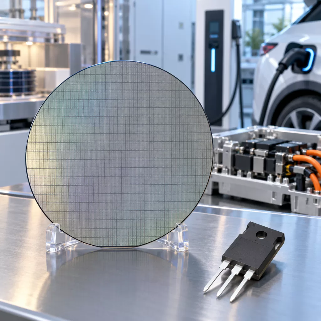
However, increasing wafer diameter from 150 mm to 200 mm is not simply a matter of producing a larger SiC crystal.
For power MOSFET fabrication, the electrical performance and yield of the finished device depend strongly on the interaction between the SiC substrate and the epitaxial layer.
Epilayer thickness, doping concentration, doping uniformity, basal plane dislocations, wafer flatness and surface quality therefore need to be specified together rather than evaluated independently.
This article explains the major requirements buyers and device engineers should consider when sourcing 8-inch SiC epitaxial wafers for 1200 V MOSFET manufacturing.
Why 200 mm SiC Matters for 1200 V MOSFET Manufacturing
150 mm SiC wafers currently remain widely used in commercial power semiconductor manufacturing, but the industry is increasingly developing 200 mm platforms.
The primary economic advantage comes from wafer area.
An 8-inch wafer provides substantially more usable area than a 6-inch wafer, allowing more dies to be fabricated in each process cycle.
In principle, this can reduce manufacturing cost per device when wafer yield, equipment utilization and process maturity are sufficiently high.
The transition also enables SiC manufacturing to take advantage of semiconductor equipment and automation infrastructure designed for larger wafer formats.
But SiC creates challenges that are less significant in conventional silicon processing.
SiC is mechanically hard, crystal growth is difficult, wafering introduces stress, and crystal defects can propagate into epitaxial layers.
As wafer diameter increases, maintaining uniformity across the entire 200 mm surface becomes more difficult.
Consequently, an 8-inch SiC wafer with acceptable average values may still create device-yield problems if local thickness, doping, crystal defects or wafer shape are poorly controlled.
Recent commercial 200 mm SiC materials have placed particular emphasis on improved doping uniformity, epitaxial thickness uniformity and reduced crystal-defect density.
Typical Structure of a 1200 V SiC MOSFET Epitaxial Wafer
A typical SiC MOSFET wafer begins with an n-type 4H-SiC substrate.
An n-type epitaxial layer is then grown on the Si-face of the substrate.
The epitaxial layer ultimately forms the voltage-supporting drift region of the device.
A simplified structure can be represented as:
Device structures
↓
N-type SiC epitaxial drift layer
↓
N+ 4H-SiC substrate
↓
Backside metal contact
For a 1200 V MOSFET, the drift-region thickness and doping concentration must be carefully balanced.
A thicker or more lightly doped drift layer can support higher blocking voltage, but it also increases electrical resistance.
A thinner or more heavily doped drift region can reduce resistance, but excessive doping may reduce breakdown capability.
The optimum specification therefore depends on the MOSFET structure and process design rather than on voltage rating alone.
Planar MOSFETs, trench MOSFETs and more advanced cell structures may use different epitaxial designs even when all devices carry a nominal 1200 V rating.
For this reason, buyers should avoid specifying only:
“200 mm SiC epi wafer for 1200 V MOSFET.”
A complete RFQ should define the substrate and epitaxial requirements separately.
1. SiC Epilayer Thickness
Epitaxial thickness is one of the most important parameters determining breakdown voltage and specific on-resistance.
For many 1200 V-class SiC MOSFET designs, the active drift layer is generally in the approximately 8–15 µm range, although the actual specification depends on device architecture, doping and required voltage margin.
The important purchasing parameter is not only nominal thickness.
Thickness uniformity across the entire 200 mm wafer is equally important.
If one section of a wafer contains a significantly thinner drift layer, the local breakdown voltage may fall.
If another region is too thick, the device may exhibit higher resistance than expected.
Therefore, the RFQ should normally specify:
Nominal epitaxial thickness
Thickness tolerance
Within-wafer thickness uniformity
Wafer-to-wafer repeatability
Measurement method
Edge exclusion
Measurement-map requirements
Commercial SiC epitaxy specifications commonly use FTIR or other calibrated thickness measurement techniques. Commercial 200 mm epi products are now available with epitaxial thicknesses extending well beyond those required for conventional 1200 V devices, illustrating the increasing maturity of large-diameter SiC epitaxy platforms.
For production qualification, a wafer map is often more useful than a single average thickness value.
2. Doping Concentration
The drift-layer doping level is directly related to the tradeoff between breakdown voltage and conduction resistance.
For n-type SiC epitaxy, nitrogen is normally used as the donor dopant.
The net donor concentration is generally expressed as:
ND − NA
where ND represents donor concentration and NA represents acceptor concentration.
For a power-device designer, two epi wafers with the same thickness may behave very differently if their net doping levels differ.
This is why an RFQ should include both:
Target net doping concentration
Acceptable doping tolerance
The customer should also clarify whether the specification refers to nominal doping, mean measured doping or a defined range across the wafer.
For more advanced device structures, the epitaxial stack may contain multiple layers rather than one uniformly doped layer.
Examples include:
buffer layers,
drift layers,
current-spreading layers,
heavily doped contact layers,
and custom multilayer epitaxial structures.
In these cases, each layer should be specified separately.
3. Doping Uniformity Across a 200 mm Wafer
Moving from 150 mm to 200 mm dramatically increases the importance of radial uniformity.
During chemical vapor deposition, gas flow, temperature distribution, precursor concentration and wafer rotation can all affect dopant incorporation.
A wafer may therefore show center-to-edge variations.
For MOSFET fabrication, poor doping uniformity can result in variations in:
breakdown voltage,
specific on-resistance,
threshold-related device characteristics,
current distribution,
and die-to-die electrical performance.
Modern 200 mm SiC epitaxy platforms are consequently placing increased emphasis on both doping and thickness uniformity.
When evaluating suppliers, buyers should ask whether doping uniformity is measured using several discrete points or supplied as a full-wafer map.
The definition also matters.
Uniformity may be reported using:
maximum-minus-minimum variation,
standard deviation,
percentage deviation from wafer mean,
or another supplier-specific calculation.
Two suppliers quoting “±10% uniformity” may therefore not necessarily be describing exactly the same measurement.
The calculation method should be agreed during qualification.
4. Why BPD Is Important
Basal plane dislocations are among the important crystallographic defects considered when producing SiC power devices.
BPDs can originate in the substrate and propagate toward or into the epitaxial layer.
During epitaxial growth, some BPDs can convert into threading edge dislocations.
Controlling this conversion and reducing BPD propagation are important aspects of high-quality SiC epitaxy.
For certain bipolar operating conditions, basal plane defects can contribute to stacking-fault expansion and electrical degradation.
Even though modern SiC MOSFETs are primarily unipolar devices, BPD control remains an important material-quality parameter because MOSFET structures include an intrinsic body diode that may conduct under particular operating conditions.
For automotive and industrial applications requiring long operating lifetimes, manufacturers therefore pay close attention to BPD-related material quality.
Recent improvements in 200 mm SiC crystal growth have also targeted reductions in BPD, TSD, micropipe and overall etch-pit densities.
5. Substrate Defects Still Matter After Epitaxy
A high-quality epitaxial layer cannot completely compensate for a poor-quality underlying substrate.
Important substrate defects include:
micropipes,
basal plane dislocations,
threading screw dislocations,
threading edge dislocations,
stacking faults,
polytype inclusions,
and other crystallographic imperfections.
The relevance of each defect type depends on device design and process flow.
Some defects directly affect device performance, while others primarily reduce the usable device area or wafer yield.
For 200 mm material, defect mapping is particularly valuable.
Instead of relying only on an average defect density, device manufacturers increasingly benefit from understanding the spatial distribution of defects across the wafer.
A wafer with the same average defect density can produce very different device yield depending on whether defects are randomly distributed or concentrated in certain regions.
6. Surface Defects Generated During Epitaxy
Not all defects originate in the SiC crystal.
Epitaxial growth can introduce its own surface defects.
Typical epi-related defects may include:
carrot defects,
triangular defects,
downfall defects,
particles,
step bunching,
scratches,
surface pits,
and other morphological abnormalities.
These defects can interfere with lithography, gate oxide formation and device active regions.
Defect inspection therefore becomes increasingly important as MOSFET die sizes increase or when manufacturers attempt to improve die yield across a 200 mm wafer.
When sourcing epi wafers, customers should clarify:
acceptable epi-defect classes,
inspection equipment,
minimum detectable defect size,
edge exclusion,
defect-map format,
and whether raw inspection data can be supplied.
Commercial SiC epi specifications may use dedicated automated inspection platforms such as Lasertec SICA for epi-defect characterization.
7. Surface Roughness
The front surface of the epitaxial wafer must support subsequent semiconductor processing.
Surface roughness influences processes such as:
gate oxidation,
photolithography,
ion implantation,
thin-film deposition,
and metallization.
AFM is commonly used to evaluate nanoscale roughness.
However, buyers should pay attention to measurement conditions.
An RFQ specifying only:
“Ra <0.5 nm”
may be incomplete.
The AFM scan area also needs to be defined, for example:
5 × 5 µm,
10 × 10 µm,
or another agreed area.
Surface-quality requirements may also include scratch criteria, pits and localized polishing damage.
8. Wafer Flatness: TTV, Bow and Warp
Wafer shape becomes increasingly difficult to control as SiC diameter increases.
For a 200 mm wafer, excessive deformation can affect:
lithography focus,
wafer chucking,
robot handling,
implantation,
film deposition,
CMP,
and downstream wafer thinning.
The three commonly requested parameters are:
TTV — Total Thickness Variation
Bow
Warp
They measure different aspects of wafer geometry and should not be treated as interchangeable.
TTV measures thickness variation.
Bow measures the displacement of the wafer’s median surface relative to a reference plane.
Warp describes the total difference between the highest and lowest points of that median surface.
For 200 mm MOSFET manufacturing, wafer shape requirements should ideally be agreed with the intended fabrication line.
A specification suitable for research epitaxy may not be sufficient for a fully automated production fab.
9. Substrate Thickness
200 mm SiC substrates must be sufficiently robust for crystal processing, epitaxy, transportation and semiconductor fabrication.
At the same time, the final power device usually requires backside thinning during fabrication.
Commercial 200 mm substrates have been introduced with thicknesses around 350 µm for advanced manufacturing platforms, although actual required thickness depends on supplier capability and fab process.
When specifying substrate thickness, buyers should include:
nominal thickness,
thickness tolerance,
TTV,
bow,
warp,
and backside surface condition.
Wafer thinning requirements should be discussed separately from incoming substrate thickness.
10. Crystal Orientation and Off-Axis Angle
Commercial power-device substrates normally use 4H-SiC.
An intentional off-axis orientation from the basal plane is commonly used to promote step-flow epitaxial growth.
For modern SiC power electronics, approximately 4° off-axis substrates are widely used.
However, the RFQ should not simply state:
“4-degree SiC wafer.”
It should define:
crystal polytype,
surface orientation,
off-axis angle,
off-axis direction,
orientation tolerance,
primary reference method,
and Si-face or C-face.
The epi surface for conventional MOSFET manufacturing is normally the Si-face.
11. Edge Exclusion
Edge exclusion becomes increasingly important with 200 mm wafers.
The extreme wafer edge may show different epitaxial thickness, doping or defect behavior compared with the central usable region.
Therefore, uniformity and defect specifications normally apply only inside a defined edge-exclusion area.
For example, commercial SiC epitaxy specifications may use a 3 mm edge exclusion for certain measurements.
When comparing quotations from different suppliers, customers should make sure the stated uniformities use the same edge-exclusion definition.
Otherwise, the numbers are not directly comparable.
12. Backside Requirements
The backside of the substrate also affects wafer handling and later device processing.
Possible specifications include:
backside roughness,
backside cleanliness,
laser marking,
wafer ID,
edge condition,
and backside polishing.
For wafers intended for power MOSFET manufacturing, later backside thinning and metallization should also be considered.
Excessive subsurface damage from earlier grinding operations can complicate downstream thinning.
13. Wafer Traceability
Traceability becomes increasingly important when a device manufacturer moves from R&D to qualification and volume production.
A wafer certificate should ideally link the finished epi wafer to:
crystal boule,
substrate lot,
wafer ID,
polishing lot,
epitaxy run,
inspection results,
and final shipment lot.
This makes it easier to analyze correlations when device yield changes.
For automotive qualification in particular, lot consistency may become as important as the performance of one exceptionally good wafer.
Recommended RFQ Parameters for 200 mm SiC Epi Wafers
A practical RFQ for 1200 V MOSFET development should contain at least the following information.
Substrate
Diameter: 200 mm / 8 inch
Material: 4H-SiC
Conductivity: N-type
Surface: Si-face
Orientation: (0001), typically off-axis for epitaxy
Off-axis angle and direction
Substrate thickness
Thickness tolerance
TTV
Bow
Warp
Resistivity range
Micropipe specification
BPD requirement
TSD/TED requirements if applicable
Surface roughness
Frontside finish
Backside finish
Edge exclusion
Epitaxy
Conductivity type
Dopant
Number of epi layers
Target epi thickness
Epi thickness tolerance
Thickness uniformity
Target net doping concentration
Doping tolerance
Doping uniformity
BPD specification
Surface-defect specification
Surface roughness
Edge exclusion
Inspection method
Wafer map requirement
Certificate of analysis
Application Information
MOSFET voltage class: 1200 V
Device structure: planar or trench
Research, qualification or production use
Target breakdown voltage
Target specific on-resistance
Expected wafer quantity
Required wafer-lot consistency
These details help the substrate and epitaxy supplier propose a material specification matched to the actual device rather than quoting a generic SiC epi wafer.
150 mm vs 200 mm SiC Epitaxy
Moving from 150 mm to 200 mm provides clear manufacturing opportunities, but the larger diameter also raises material requirements.
A 200 mm epi wafer must maintain acceptable performance over approximately 1.78 times the area of a 150 mm wafer.
That means suppliers must control:
thermal gradients,
gas distribution,
epitaxy growth rate,
dopant incorporation,
crystal stress,
wafer shape,
and defect distribution
over a significantly larger surface.
This is why a nominally correct thickness and doping concentration are no longer enough.
The real challenge is wafer-scale uniformity.
For device manufacturers, 200 mm material qualification should therefore emphasize mapping data and statistical lot consistency rather than only center-point measurements.
Should Every 1200 V MOSFET Project Move to 200 mm?
Not necessarily.
150 mm SiC remains a practical choice for many production and development programs.
A transition to 200 mm makes the most sense when the complete manufacturing ecosystem supports the larger wafer format.
This includes:
substrate availability,
epitaxy,
implantation,
oxidation,
lithography,
etching,
metallization,
wafer thinning,
inspection,
testing,
and packaging.
For early-stage device development or specialty devices with relatively low wafer volume, 150 mm material may still be economically attractive.
For higher-volume manufacturing, however, 200 mm SiC offers an important path toward improved manufacturing scale and potentially lower device cost.
Conclusion
The development of 8-inch SiC manufacturing is changing the way 1200 V MOSFET producers evaluate substrate and epitaxial materials.
The key question is no longer simply whether a supplier can produce a 200 mm SiC wafer.
The more important questions are:
Can epilayer thickness remain uniform across 200 mm?
Can net doping remain stable from center to edge?
Can substrate BPD propagation be controlled?
Can epi surface defects be kept outside critical device regions?
Can TTV, bow and warp meet automated fab requirements?
Can the same material quality be repeated from lot to lot?
For 1200 V SiC MOSFET production, substrate quality, epitaxy quality and wafer-scale uniformity ultimately need to be considered as one material system.
A detailed RFQ covering epitaxial thickness, doping, defect density, wafer geometry and inspection requirements can significantly reduce qualification risk and make comparisons between SiC wafer suppliers more meaningful.