
customizable Ti doped sapphire windows,Titanium sapphire windows Ti:Sapphire 0.5mm thickness or ultra-thin

Ti doped sapphire windows’ abstract Ti doped sapphire windows’ properties Absorption range 400 – 600 nm Tuning range 660 – 1050 nm Emission peak 795 nm Absorption peak 488 nm Absorption cross-section at peak wavelength 38×10-20 cm2 Emission Cross-section Σ532nm = 4.9 x 10⁻²⁰ cm2 Emission Cross-section Σ490nm = 6.4 x 10⁻²⁰ cm2 Emission cross-section Σ790nm […]
Single crystal sapphire ingot 80 200 400kg,CZ KY growth method for sapphire finishing processes.

Single crystal sapphire ingot’s abstrtact Single crystal sapphire ingot’s properties Chemical formula Al2O3 Crystal class Hexagonal system, rhomboidal class 3m Lattice constants, A a=4.785, c=12.991 Density, g/cm3 3.98 Melting point, °K 2303 Hardness Knoop(daN/mm2): 1800 parallel to C-axis, 2200 perpendicular to C-axis, Mohs: 9 Optical transmission range, µm 0.17 – 5.5 Refractive index at 0.532 […]
200mm 8inch sic wafer 4H-N 6H-N type thickness of 350um-500um 8inch Silicon Carbide Wafers & SiC Epitaxy

8inch Silicon Carbide Wafers‘ abstract The abstract for 8-inch Silicon Carbide Wafers should extensively detail the type and grade of8inch sic wafer, covering various aspects such as specific types like 4H-SiC or 6H-SiC, and different grades like commercial or high-purity grade. Additionally, it should provide a comprehensive overview of additional specifications relevant to application or […]
8inch SiC wafer Silicon Carbide Wafer prime dummy research grade 500um 350 um
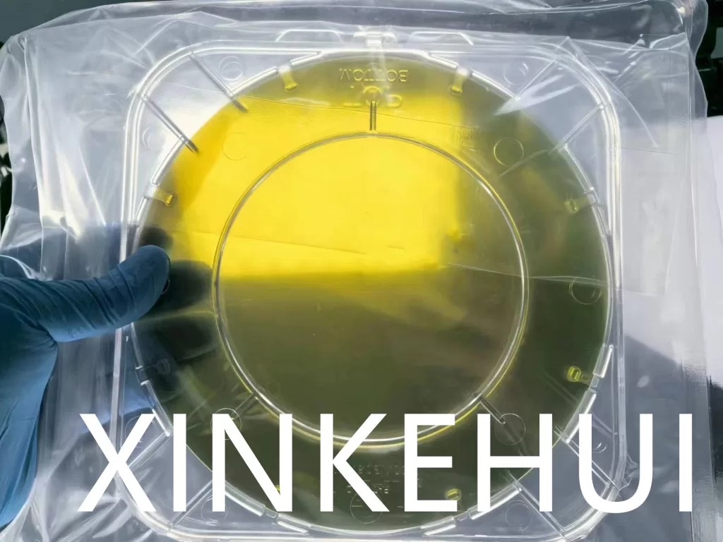
8inch SiC wafer’s abstract 8-inch SiC wafers are increasingly gaining popularity and demand in various industries. As the market for SiC wafers expands, there is a growing need for these high-quality substrates to support research, development, and commercial applications. With their exceptional properties and wide-ranging potential, 8-inch SiC wafers are becoming the preferred choice for […]
sapphire ingot Al2O3 80kg 200kg 400kg KY CZ for industrial sapphire component the origin of sapphire production
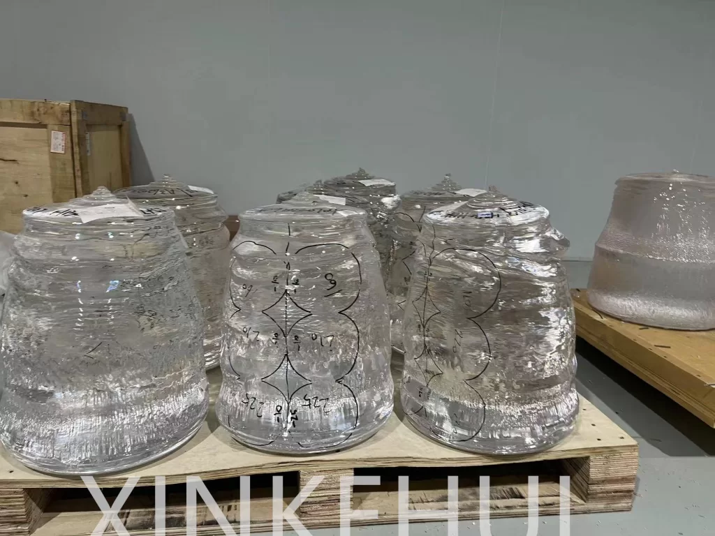
Sapphire ingot‘s abstract Sapphire ingot‘s showcase Sapphire ingot‘s applications Sapphire ingot‘s feature The advantages of our company in sapphire ingot production Crafted with precision from aluminum oxide crystals, our sapphire ingots are the cornerstone of high-quality sapphire substrate production. Engineered with a keen focus on performance optimization, our ingots are tailored to meet the diverse […]
InP wafers VGF CZ Growth method N-type S doped P type Zn doped EPI-ready 2、3、4、6inch semiconductor materials
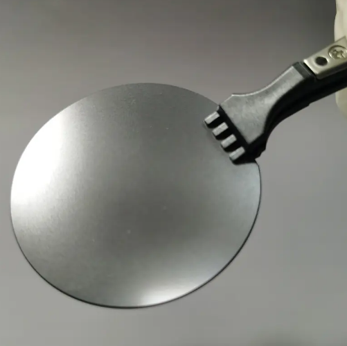
InP wafers’ abstract InP wafers’ properties InP wafers’ data chart(partly) Type Semi-Insulated N-Type P-Type NP Type Dopant Fe S, Sn Zn Undoped Growth Method VGF Diameter 2″, 3″, 4″, 6″ Orientation (100)±0.5° Thickness (µm) 350-675um ±25um OF/IF US EJ Carrier Concentration – (0.8-8)*1018 (0.8-8)*1018 (1-10)*1015 Resistivity (ohm-cm) >0.5*107 – – – Mobility (cm2/V.S.) >1000 1000-2500 […]
exceptional Silicon Wafer, Type P N,2inch 4inch 6inch 8inch,Single side polish Epi ready (Customizable)

Silicon Wafer’s abstract Silicon Wafer’s showcase Silicon Wafer’s properties(partly) Silicon Wafer’s application Manufacturing Process Silicon wafers are crucial components in the manufacturing process of electronic devices such as cell phones, TVs, computers, and smart speakers. These wafers are thin slices of pure crystallized silicon, often referred to as undoped or intrinsic silicon wafers. One of […]
Sapphire Glass Ball Lens Premium Product Dia 3-0.25mm Applied in cutting-edge medical technology

Sapphire Glass Ball Lens‘ abstract Introducing our Sapphire Glass Ball Lens, a revolutionary component poised at the forefront of cutting-edge medical technology. Crafted with precision and durability in mind, thisSapphire Glass Ball Lens stands as a beacon of innovation, enhancing the capabilities of medical devices across various applications. Designed to meet the exacting demands of […]