
Opis
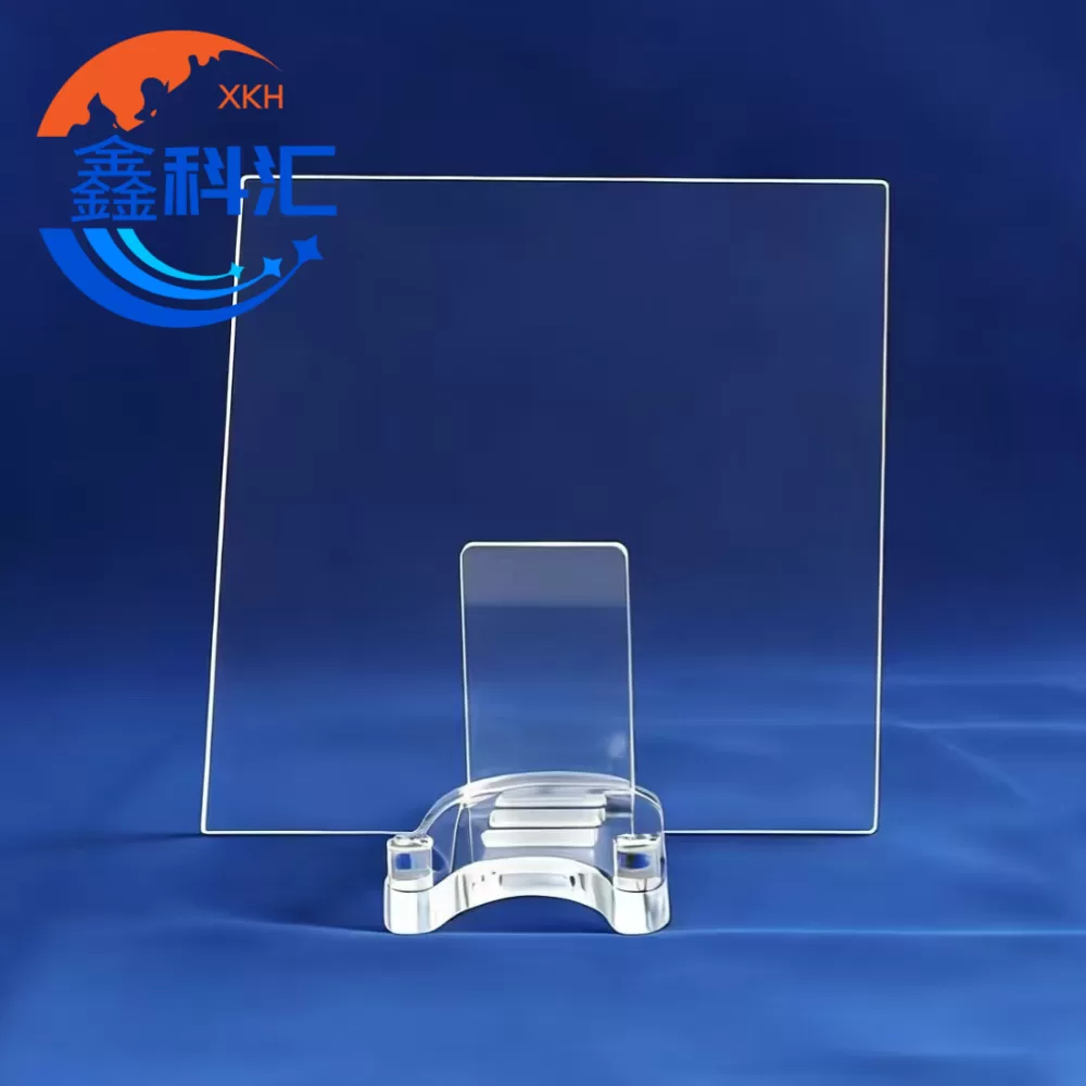
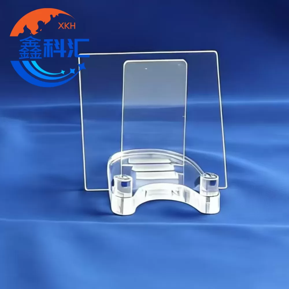
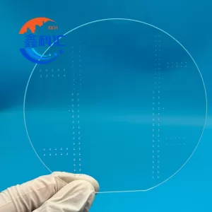
The 310 × 310 × 1 mm Large-Area Square Sapphire Substrate is a precision-engineered sapphire plate produced from high-purity single-crystal aluminum oxide (Al₂O₃). Designed for applications that exceed the dimensional limits of conventional sapphire wafers, this ultra-large substrate provides excellent flatness, thermal endurance, and mechanical integrity across a square geometry.
This product is not a standard semiconductor wafer. Instead, it is optimized as a functional sapphire substrate or carrier plate for semiconductor processing, optical systems, and aerospace environments where large surface area, dimensional stability, and resistance to extreme conditions are required.
Typowe przypadki użycia
Carrier and support substrates for semiconductor processing
GaN-on-Sapphire epitaxial carrier plates
Large-area optical and laser windows
High-temperature or vacuum viewports
Structural sapphire base plates
Research and custom industrial platforms
Specyfikacja techniczna
| Parametr | Specyfikacja |
|---|---|
| Materiał | Single Crystal Sapphire (Al₂O₃) |
| Crystal Purity | ≥ 99.99% |
| Geometry | Square |
| Overall Dimensions | 310 × 310 mm |
| Nominal Thickness | 1.0 mm |
| Tolerancja grubości | ± 0.02 mm |
| Total Thickness Variation (TTV) | < 10 μm |
| Orientacja kryształu | C-Plane (0001) |
| Surface Processing | Double-Side Polished (DSP) |
| Chropowatość powierzchni | Ra < 0.2 nm |
| Płaskość powierzchni | λ/10 @ 633 nm |
| Edge Treatment | Chamfered / Radius Corners |
| Optical Grade | High Optical Quality |
| Twardość | Mohs 9 |
| Gęstość | 3,98 g/cm³ |
| Przewodność cieplna | ~35 W/m·K (25 °C) |
| Maximum Service Temperature | > 1600 °C |
| Stabilność chemiczna | Excellent resistance to acids and alkalis |
Performance Advantages
Large-Area Dimensional Stability
Maintains high flatness and tight thickness control across a 310 mm square surface, enabling reliable use in large-format systems.
High Mechanical Strength
The intrinsic hardness and strength of sapphire reduce the risk of surface damage and deformation during handling and operation.
Thermal Endurance
Capable of sustaining high-temperature cycles typical of epitaxial growth, thermal processing, and aerospace environments.
Optical-Grade Surface Finish
Sub-nanometer surface roughness enables use in optical transmission, bonding, and precision alignment applications.
Chemical Inertness
Superior resistance to corrosive gases, acids, and alkalis compared with glass or fused quartz substrates.
Manufacturing & Inspection
Synthetic sapphire crystal growth
Precision cutting and stress-relief processing
Large-format double-side polishing
Interferometric flatness measurement
Full dimensional and visual inspection prior to shipment
Frequently Asked Questions
Q1: How should this product be classified?
This product is classified as a large-area sapphire substrate or carrier plate, not a standard semiconductor wafer.
Q2: Are other sizes or thicknesses available?
Yes. Custom square or rectangular dimensions from 250 mm to 310 mm per side and various thicknesses are available upon request.
Q3: Is this suitable for GaN epitaxial processing?
Yes. It is commonly used as a GaN-on-Sapphire carrier substrate in MOCVD and related epitaxial systems.
Q4: How is surface flatness verified?
Each substrate is measured using laser interferometry to ensure λ/10 flatness at 633 nm.
Q5: How is the substrate protected during shipping?
Products are packed in custom shock-absorbing, clean-grade packaging designed specifically for ultra-large sapphire components.

Opinie
Na razie nie ma opinii o produkcie.