
As electric vehicles, renewable energy systems, industrial drives, and high-power electronics continue evolving toward higher efficiency and power density, Silicon Carbide (SiC) power semiconductors have moved from emerging technology into large-scale commercialization.
Compared with traditional silicon (Si) devices, SiC MOSFETs deliver higher switching speeds, lower losses, and superior high-temperature capability. However, their material structure and operating conditions introduce reliability challenges that differ fundamentally from conventional silicon technology.
For engineers and manufacturers, understanding SiC reliability is no longer optional—it directly impacts system lifetime, field failure rates, and long-term operating cost.
This article explores the physical characteristics of SiC, explains why reliability testing requires additional considerations, and examines defect origins, failure mechanisms, and reliability evaluation methods.
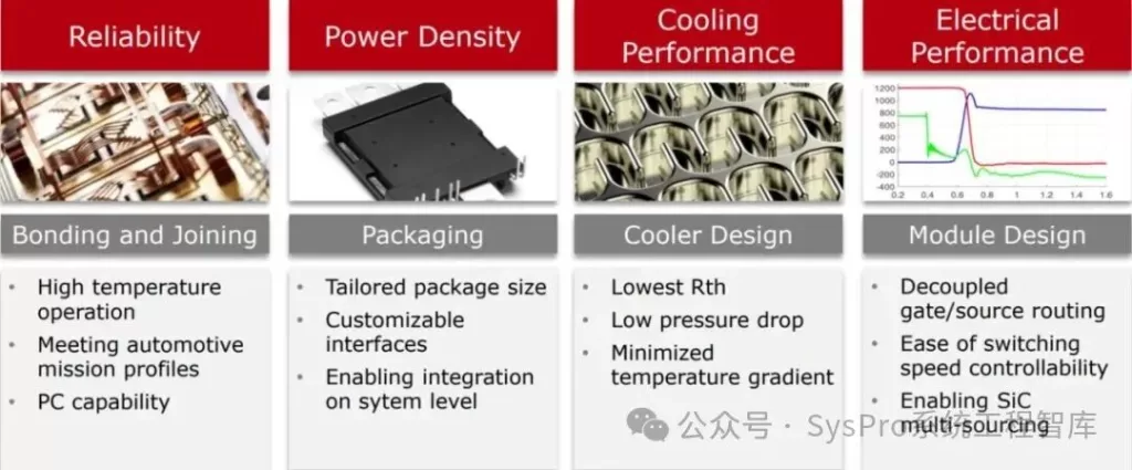
Why Reliability Matters More for SiC Power Devices
Traditional silicon-based power devices have benefited from decades of manufacturing optimization. Their failure mechanisms and lifetime models are well established.
SiC devices, however, operate under much harsher conditions:
- Higher electric fields
- Faster switching rates
- Increased junction temperatures
- Greater power density
- More demanding thermal cycling
These advantages improve performance but also create new stress mechanisms.
Unlike silicon technology, many reliability concerns in SiC originate not only from device design but also from material-level defects and interface behavior.
Fundamental Physical Properties of SiC
Silicon Carbide possesses several physical advantages over conventional silicon.
| Property | Silicon (Si) | Silicon Carbide (SiC) |
|---|---|---|
| Bandgap | ~1.1 eV | ~3.2 eV |
| Breakdown Electric Field | ~0.3 MV/cm | ~3 MV/cm |
| Thermal Conductivity | Moderate | High |
| Electron Saturation Velocity | Lower | Higher |
| Maximum Operating Temperature | Limited | Much higher |
These material properties enable:
- Higher voltage operation
- Reduced conduction loss
- Faster switching performance
- Smaller device size
- Improved thermal management
This explains why SiC MOSFETs increasingly replace IGBTs in EV inverters, charging systems, photovoltaic converters, and industrial applications.
How SiC Material Characteristics Influence Device Reliability
While SiC provides substantial performance improvements, several material properties create additional complexity.
Crystal Anisotropy
SiC exhibits directional properties. Physical and electrical characteristics vary with crystal orientation.
As a result:
- Manufacturing windows become narrower
- Process consistency becomes more difficult
- Interface behavior varies with crystal direction
This anisotropic nature can affect long-term reliability.
More Complex Defect Structures
Compared with silicon, SiC crystal growth is more difficult.
Typical defects include:
- Basal Plane Dislocations (BPD)
- Threading dislocations
- Micropipes
- Stacking faults
- Epitaxial defects
These crystal imperfections may create localized electric field enhancement and degrade reliability.
Even a small defect density can influence yield and device lifetime.
SiC–SiO₂ Interface Challenges
One of the largest differences between Si and SiC MOS devices lies at the gate oxide interface.
Although SiC MOSFETs still use silicon dioxide (SiO₂) gate insulation, the SiC/SiO₂ interface naturally generates:
- Higher interface trap density
- Mobility degradation
- Charge trapping effects
- Threshold voltage instability
This interface remains one of the most studied reliability topics in SiC technology.
Gate Oxide Reliability: The Critical Challenge in SiC MOSFET Commercialization
For many years, gate oxide reliability was considered one of the major barriers preventing widespread SiC adoption.
The gate oxide performs two essential functions:
- Electrical insulation
- Formation of MOS channel control
Its quality directly affects:
- Switching behavior
- Channel mobility
- Threshold voltage stability
- Device lifetime
If gate oxide integrity degrades, early failure becomes increasingly likely.
Why Gate Oxide Reliability Receives Special Attention
SiC MOSFETs often operate at:
- Electric fields significantly higher than silicon devices
- Blocking voltages above 1000V
- Switching speeds exceeding tens of volts per nanosecond
These conditions expose the gate oxide to severe stress.
Unlike standard silicon MOS devices, SiC devices may experience:
- Long-term charge trapping
- Oxide wear-out
- Threshold drift
- Time-dependent dielectric breakdown (TDDB)
Therefore conventional silicon qualification methods alone are insufficient.
Additional reliability tests are typically required.
Origin of Gate Oxide Defects
The intrinsic dielectric strength of SiO₂ itself is not dramatically worse on SiC.
The problem often comes from external defects.
Examples include:
Physical oxide thinning
Possible causes:
- Epitaxial defects
- Substrate irregularities
- Surface morphology distortion
Electrical oxide thinning
Possible causes:
- Metallic contamination
- Particles
- Voids
- Process-induced impurities
These microscopic defects create localized weak regions inside the oxide.
Under high electric field stress, these weak points become preferred failure sites.
They effectively behave like tiny “weak spots” in the gate dielectric.
How Manufacturers Control SiC Gate Oxide Defects
Modern SiC manufacturers implement multiple layers of screening and process control.
Common strategies include:
Material quality optimization
- Improved substrate growth
- Reduced crystal defects
- Better epitaxial layer control
Interface engineering
Methods may include:
- Nitrogen annealing
- Interface passivation
- Optimized oxidation recipes
Statistical screening approaches
Manufacturers often apply stress-based screening techniques to remove weak devices before shipment.
This acts like a filtering mechanism that identifies latent oxide defects.
Only devices passing reliability criteria proceed to mass production.
Measuring SiC MOSFET Failure Probability
Estimating failure probability under normal operating conditions presents a major challenge.
Direct lifetime testing under nominal stress could require decades.
Therefore accelerated stress techniques are widely used.
Two common approaches are discussed below.
1. Long-Duration Constant Stress Testing
This method applies elevated:
- Temperature
- Voltage
- Electric field stress
for extended periods.
Purpose:
- Accelerate degradation
- Observe early failures
- Estimate long-term reliability
The principle is similar to a marathon endurance test.
Devices operate continuously under severe conditions until degradation mechanisms emerge.
2. Step-Stress Gate Voltage Testing
In this approach, gate voltage gradually increases in steps.
Engineers monitor:
- Leakage current
- Threshold voltage
- Breakdown behavior
- Device degradation trends
Advantages:
- Faster statistical data collection
- Identification of weak populations
- Improved screening methodology
The resulting data can support Weibull analysis and lifetime prediction models.
Weibull Distribution and Reliability Modeling
Reliability engineers frequently use Weibull statistical analysis to estimate failure behavior.
The Weibull model helps predict:
- Early-life failures
- Random failures
- Wear-out failures
For SiC MOSFET gate oxide evaluation, Weibull plots can reveal:
- Defect density
- Process consistency
- Reliability improvements over generations
Modern SiC devices show significant improvement compared with earlier technology generations.
Future Outlook
SiC technology has progressed dramatically over the last decade.
Improvements in:
- Crystal growth
- Oxidation processes
- Interface treatment
- Defect screening
- Reliability qualification
have transformed SiC from a laboratory technology into a mature commercial solution.
However, reliability remains a major engineering focus.
As voltage ratings and switching frequencies continue increasing, understanding and controlling failure mechanisms will become even more important.
Companies investing in SiC manufacturing and applications should consider reliability engineering not as a final verification step, but as an integral part of design and production.
FAQ
Why do SiC MOSFETs require extra reliability testing compared with silicon devices?
SiC devices operate under higher electric fields, faster switching conditions, and more demanding thermal environments. Their unique material characteristics introduce failure mechanisms not commonly seen in traditional silicon technology.
What is the biggest reliability challenge in SiC MOSFETs?
Gate oxide reliability is widely considered one of the most critical challenges. Interface defects and charge trapping can significantly influence threshold stability and long-term device lifetime.
How do manufacturers reduce SiC device failure rates?
Manufacturers improve crystal quality, optimize oxidation processes, implement interface passivation techniques, and use stress-based screening methods to remove weak devices before shipment.